Diagnostic Testing and Troubleshooting (2635A)
Digital and Alarm Output Troubleshooting
5A
5A-21
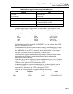
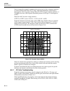
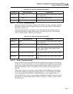
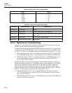
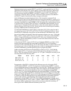
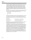
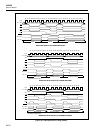
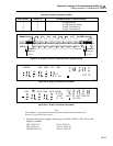
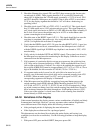
Figure 5A-7 shows the timing relationships of the MC68302 Microprocessor address,
data, and memory control signals used for memory read and write cycles. The chip
selects from the Microprocessor (FLASH*, SRAM*, XMCARD*, and I/O*) are decoded
internally from the address bus and the address strobe (AS*) signal. Therefore the AS*
waveform is the same as the chip select signal for the device that the Microprocessor is
accessing.
If the instrument powers up without any errors, but does not recognize front-panel button
presses, the problem may be in the Keyboard Interrupt (KINT*) signal from the FPGA.
If the KINT* output (A1U25-62) is low (and never goes high), the Microprocessor
(A1U1) is failing to recognize the interrupt, or the microprocessor interface to A1U25 is
not working correctly. Verify that the KINT* signal gets to the input pin (A1U1-121) on
the Microprocessor.
If the interval time does not count down properly when scanning is enabled, the problem
may be in the Real-Time Clock Interrupt (CINT*) signal from the Real-Time Clock
(A1U12). If the CINT* output (A1U12-3) is low (and never goes high), the
Microprocessor (A1U1) is failing to recognize the interrupt or the microprocessor
interface to A1U12 is not working correctly. Verify that the CINT* signal gets to the
input pin (A1U1-96) on the Microprocessor. Also verify that the Real-Time Clock is
actively keeping time by checking for a 1-Hz square wave output on A1U12-4. Pin
A1U12-2 must also be properly connected to GND for the Real-Time Clock to operate.
The interface to the Microprocessor operates very much like the interface to NVRAM
device A1U20.
5A-15. Digital and Alarm Output Troubleshooting
Power up Hydra while holding down the CANCL button to reset the instrument
configuration. Since the structure of the eight Digital Outputs and four Alarm Outputs is
very similar, the troubleshooting procedure presented here does not refer to specific
device and pin numbers. First verify that the input of the Output Driver (A1U17 or
A1U27) is low and that the output is near +5V dc. If the input is high, the problem may
be in the FPGA (A1U25). If the output is not near +5V dc, use an ohmmeter to check the
pull-up resistor in A1Z2.
Use the proper computer interface command to change the state of the Digital Output
(DO_LEVEL x,1) or Alarm Output (ALARM_DO_LEVEL x,1), where x is the number
of the output being checked. Now verify that the input of the Output Driver is high and
that the output is near +0.8V dc. If there is no change in the input, check the address
signals to the FPGA (A1U25-85, A1U25-90, A1U25-96, A1U25-97) and the behavior of
the output pin on the FPGA that goes to the input of the Output Driver (A1U17 or
A1U27). If the output of the Output Driver fails to change when the input does, the
problem is most likely the inverting output driver (A1U17 or A1U27).
5A-16. Digital Input Troubleshooting
Power up Hydra while holding down the CANCL button to reset the instrument
configuration. Verify that the Input Buffer Threshold circuit generates approximately
1.4V dc at A1TP18. Drive the Digital Input (A1J5) to be checked with a signal generator
outputting a 100-Hz square wave that transitions from 0 to +5V dc. The signal generator
output common should be connected to Common (A1J5-1). Verify that the output of the
Input Buffer is a 100-Hz square wave that is the inverse of the input signal.


