


Diagnostic Testing and Troubleshooting (2635A)
Digital Kernel Troubleshooting
5A
5A-19
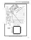
During instrument power-up, the RESET* and HALT* signals are held low for 140 to
280 milliseconds after the VCC power supply is greater than 4.65 volts dc. Before the
Microprocessor can begin execution of the firmware stored in the Flash Memory, the
reset circuit must release the RESET* and HALT* signals (A1U2-11 and A1U2-8
respectively) and allow them to go high. Verification of the operation of the RESET*
and HALT* signals is best done by using a storage oscilloscope.
After the Microprocessor has begun execution of the instructions stored in Flash
Memory (A1U14 and A1U16), the Microprocessor may drive the HALT* signal (A1U1-
91) low if the instructions executed are not correct. Another sign of incorrect instruction
execution is the Bus Error signal (BERR*;A1U1-94) going low to indicate that an access
to an unused area of memory space was done. To troubleshoot these problems, use an
oscilloscope to check the activity of the address, data, and control signals to the Flash
Memory devices (A1U14 and A1U16). It may also be useful to check signal continuity
by using a DMM with the instrument power off.
To check the Flash Memory control signals, verify that A1U1-128 is going low and is
also appearing on pins A1U14-22 and A1U16-22 of the Flash Memory devices. It may
be necessary to continually reset (power on) the instrument to check these lines, since
the activity probably halts quickly when the instrument software goes awry. Verify that
RDU* (A1U11-14 and A1U14-24) goes low when A1U1-128 is low. Verify that RDL*
(A1U11-19 and A1U16-24) goes low when A1U1-128 is low. If all this is true, the
problem is with the Flash Memory or there is a fault in the address/data lines from the
MC68302 Microprocessor.
Verify that the XINIT* output (A1U25-65) goes high after RESET* goes high. Verify
that the mode pins and extra chip select input on the FPGA (A1U25) are properly
connected to VCC and GND. Pins 6, 29, 54, and 56 must be about 5 volts dc. Pins 52 and
93 must be near 0 volts dc. If the Microprocessor is able to correctly fetch instructions
from the Flash Memory, the Microprocessor tries to program the FPGA.
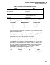
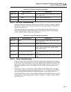
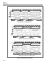
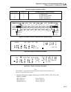
Address decoding for I/O devices like the FPGA is done by A1U11. Verify that the
PGA* output (A1U11-12) goes low when the Microprocessor attempts to access the
FPGA. Verify the address and I/O* inputs to A1-U11 (pins 2 through 8) according to the
decoding shown in the following table.
Output A<12> A<11> A<10> A<9> A<8> A<7> I/O*
PGA* (A1U11-12)
RTC* (A1U11-16)
OPTE* (A1U11-12)
0
0
0
0
0
0
0
0
0
0
0
0
0
0
1
0
1
0
0
0
0
Programming of the FPGA is initiated by the Microprocessor by driving the XD/P*
(A1U25-80) and RESET* (A1U25-78) signals low simultaneously. RESET* is pulsed
low by the Microprocessor for approximately 10 microseconds. The Microprocessor then
waits for XINIT* (A1U25-65) to go high; if this doesn’t happen, the Watchdog Timer in
the Microprocessor will reset the instrument after several seconds by driving POR*
(A1U1-117) low. Verify that the Microprocessor waits until XRDY (A1U25-99) is high
before writing each byte to the FPGA. (A1U25-88 and A1U25-5 both go low during the
write cycle.) Check the XD/P* signal (A1U25-80) at the end of the FPGA programming;
if it doesn’t go high, the Microprocessor will repeat the FPGA programming sequence
until it works correctly or the Watchdog Timer in the Microprocessor resets the
instrument by driving POR* (A1U1-117) low. If FPGA programming is failing, check
the D<8> through D<15>, PGA*, WRU*, XINIT*, XRDY, XD/P*, and RESET* signals
for activity with an oscilloscope. It may also be necessary to check the continuity of
these signals with a DMM when the instrument power is off.