


Theory of Operation (2620A/2625A)
Detailed Circuit Description
2
2-11
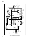
The Microprocessor communicates to the Microcontroller on the A/D Converter PCA
(via the Serial Communication circuit) using an asynchronous communication protocol
at 4800 baud. Communication to the Microcontroller (A3U9) originates at A1U4-11.
Communication from the A/D’s Microcontroller to the Microprocessor appears at A1U4-
10. When there is no communication in progress between the Microprocessor and the
Microcontroller, both of these signals are low.
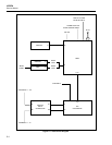
2-34. Address Decoding
The upper three bits of the address bus are decoded by A1U10-3,4,5 to generate the
ROM* chip select signal for the ROM (A1U10-6).
The NVRAM/Clock chip select signal (A1U21-6 going low) is generated when the
ROM* and RESET* signals are high and any one of address bits 9 through 12 is high.
To avoid spurious write cycles during power cycling, the INT* output of the NVRAM
(A1U3-1) is used to discharge the reset circuit on the Display PCA through resistor
A1R63 when the power supply level at A1U3-28 is too low (less than approximately
4.65V dc) to allow memory operations to the NVRAM.
The miscellaneous I/O chip select (hexadecimal addresses 0000 through 01FF) is
decoded using the ROM* signal and address bits 9 through 12 by A1U15 and A1U21.
When ROM* is high and all four of the address bits are low, the I/O* signal (A1U21-8)
is low. The I/O* signal and address bits 3 through 8 are then used by A1U10 and A1U11
to generate the CNTR*, DIO*, IEEE*, and MEM* chip select signals.
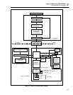
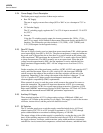
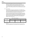
Table 2-1 shows a memory map for the Microprocessor.
Table 2-1. Microprocessor Memory Map
Hexadecimal Address Device Selected
2000 - FFFF ROM (A1U8)
1FF8 - 1FFF Real-Time Clock (A1U3)
0200 - 1FF7 NVRAM (A1U3)
0040 - 013F Microprocessor Internal RAM
0038 - 003F Counter/Timer (A1U2)
0032 (Read Only) Digital Inputs (A1U13)
0032 (Write Only) Digital Outputs (A1U26)
0035 (Write Only) Alarm Outputs (A1U16)
0028 - 002F IEEE-488 Option (2620A Only)
0005 - 0006 (Write Only) Memory Page (2625A Only)
0004 Memory Data (2625A Only)
2-35. Serial Communication (Guard Crossing)
The transmission of information from the Microprocessor (A1U4) to the Microcontroller
(A3U9) is accomplished via the circuit made up of A1U15, A1U7, A1R8, A1R16, and
A3R8. The transmit output from the Microprocessor (A1U4-11) is inverted by A1U15,
which drives the optocoupler LED (A1U7-2). Resistor A1R8 limits the current through
the LED.
The phototransistor in A1U7 responds to the light emitted by the LED when A1U7-2 is
driven low (the collector of the phototransistor (A1U7-5) goes low.) The phototransistor
collector is pulled up by A3R8 on the A/D Converter PCA. When turning off, the