


HYDRA
Service Manual
2-12
phototransistor base discharges through A1R16. With this arrangement, the rise and fall
times of the phototransistor collector signal are nearly symmetrical.
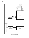
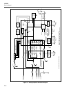
The transmission of data from the Microcontroller (A3U9) to the Microprocessor
(A1U4) is accomplished via the circuit made up of A3Q1, A3R7, A1U5, A1R7, and
A1R3. The transmit output from the Microcontroller (A3U9-14) is inverted by A3Q1,
which drives the optocoupler LED (A1U5-2) through resistor A3R7. The current through
the LED is limited by resistor A3R7. The phototransistor in A1U5 responds to the light
emitted by the LED when A1U5-2 is driven low; the emitter of the phototransistor
(A1U5-4) goes high. The phototransistor collector (A1U5-5) is pulled up by VCC, and
the emitter is pulled down by resistor A1R3. When turning off, the phototransistor base
discharges through A1R7. With this arrangement, the rise and fall times of the
phototransistor collector signal are nearly symmetrical.
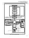
2-36. Display/Keyboard Interface
The Microcontroller sends information to the Display Processor via a three-wire
synchronous communication interface. The detailed description of the DISTX, DISRX,
and DSCLK signals may be found in the detailed description of the Display PCA. Note
that the DISRX signal is pulled down by resistor A1R1 so that Microprocessor input
A1U4-15 is not floating at any time. The Display PCA also provides the system reset
circuitry and watchdog timer.
The Keyboard interface is made up of six bidirectional port lines from the
Microcontroller. SWR1 through SWR6 (A1U4-21 through A1U4-26, respectively) are
pulled up by A2Z1 on the Display PCA. The detailed description of the Display PCA
describes how the Microprocessor interfaces to the Keyboard.
2-37. ROM
The ROM provides the instruction storage for the Microprocessor. The chip select for
this device (A1U8-20) goes low for any memory cycle between hexadecimal addresses
2000 and FFFF (accessing 56 kbytes). Whenever this device is chip selected for read, the
instruction in the addressed location is output to the data bus and read by the
Microprocessor.
2-38. NVRAM/Clock
The NVRAM/Clock (A1U3) provides the data storage and real-time clock for the
instrument. A lithium battery, a crystal, and an automatic power-fail control circuit are
also integrated into this single package. When the RAM* chip select signal (A1U3-20) is
low, the Microprocessor is accessing one of the 8192 bytes in the NVRAM/Clock. The
RD* (A1U3-22) and WR* (A1U3-27) signals go low to indicate a read or write cycle,
respectively.
The internal power-fail control circuit disables access to this device and drives the INT*
output (A1U3-1) low when the VCC power supply is below approximately +4.5V dc.
This action keeps locations in the NVRAM/Clock from being modified while the
instrument is powering up and down. When the INT* output is low, the reset circuit on
the Display PCA is discharged, and a system reset occurs. Therefore, the Microprocessor
is reset on power failure as soon as it can no longer access the NVRAM/Clock.
The NVRAM contains 8184 bytes of nonvolatile data storage. The nonvolatile
instrument configuration information, the nonvolatile measurement data, and the
Microprocessor temporary data are stored in this area.
The Clock is composed of 8-byte wide registers that allow access to the real-time clock
counters. The Microprocessor accesses these registers in the same way as the NVRAM.