System Control Coprocessor
ARM DDI 0363E Copyright © 2009 ARM Limited. All rights reserved. 4-35
ID013010 Non-Confidential, Unrestricted Access
4.2.14 c0, Cache Size Selection Register
The Cache Size Selection Register holds the value that the processor uses to select the Current
Cache Size Identification Register to use.
The Cache Size Selection Register is:
• a read/write register
• accessible in Privileged mode only.
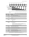
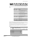
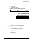
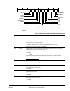
Figure 4-26 shows the bit arrangement for the Cache Size Selection Register.
Figure 4-26 Cache Size Selection Register format
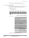
Table 4-22 shows how the bit values correspond with the Cache Size Selection Register.
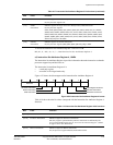
To access the Current Cache Size Identification Registers read or write CP15 with:
MRC p15, 2, <Rd>, c0, c0, 0 ; Read Cache Size Selection Register
MCR p15, 2, <Rd>, c0, c0, 0 ; Write Cache Size Selection Register
4.2.15 c1, System Control Register
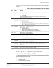
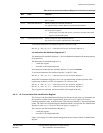
The System Control Register provides control and configuration information for:
• memory alignment, endianness, protection, and fault behavior
• MPU and cache enables and cache replacement strategy
• interrupts and the behavior of interrupt latency
• the location for exception vectors
• program flow prediction.
The System Control Register is:
• a read/write register
• accessible in Privileged mode only.
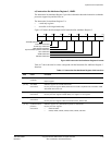
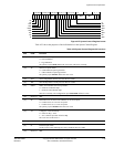
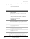
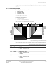
Figure 4-27 on page 4-36 shows the arrangement of bits in the register.
Reserved Level
43 10
InD
31
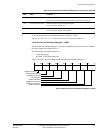
Table 4-22 Cache Size Selection Register bit functions
Bits Field Function
[31: 4] Reserved SBZ.
[3:1] Level Identifies which cache level to select.
b000 = Level 1 cache
This field is read only, writes are ignored.
[0] InD Identifies instruction or data cache to use.
1 = instruction
0 = data.


