


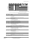
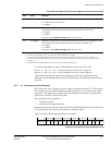

System Control Coprocessor
ARM DDI 0363E Copyright © 2009 ARM Limited. All rights reserved. 4-40
ID013010 Non-Confidential, Unrestricted Access
[17] RSDIS Return stack disable:
0 = Normal return stack operation. This is the reset value.
1 = Return stack disabled.
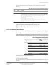
[16:15] BP This field controls the branch prediction policy:
b00 = Normal operation. This is the reset value.
b01 = Branch always taken.
b10 = Branch always not taken.
b11 = Reserved. Behavior is Unpredictable if this field is set to b11.
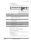
[14] DBWR Disable write burst in the AXI master:
0 = Normal operation. This is the reset value.
1 = Disable write burst optimization.
[13] DLFO Disable linefill optimization in the AXI master:
0 = Normal operation. This is the reset value.
1 = Limits the number of outstanding data linefills to two.
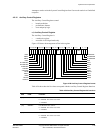
[12]
ERPEG
c
Enable random parity error generation:
0 = Random parity error generation disabled. This is the reset value.
1 = Enable random parity error generation in the cache RAMs.
Note
This bit controls error generation logic during system validation. A synthesized ASIC
typically does not have such models and this bit is therefore redundant for ASICs.
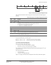
[11] DNCH Disable data forwarding for Non-cacheable accesses in the AXI master:
0 = Normal operation. This is the reset value.
1 = Disable data forwarding for Non-cacheable accesses.
[10] FORA Force outer read allocate (ORA) for outer write allocate (OWA) regions:
0 = No forcing of ORA. This is the reset value.
1 = ORA forced for OWA regions.
[9] FWT Force write-through (WT) for write-back (WB) regions:
0 = No forcing of WT. This is the reset value.
1 = WT forced for WB regions.
[8] FDSnS Force D-side to not-shared when MPU is off:
0 = Normal operation. This is the reset value.
1 = D-side normal Non-cacheable forced to Non-shared when MPU is off.
[7] sMOV sMOV of a divide does not complete out of order. No other instruction is issued until the
divide is finished.
0 = Normal operation. This is the reset value.
1 = sMOV out of order disabled.
[6] DILS Disable low interrupt latency on all load/store instructions.
0 = Enable LIL on all load/store instructions. This is the reset value.
1 = Disable LIL on all load/store instructions.
[5:3] CEC Cache error control for cache parity and ECC errors.
See Table 8-2 on page 8-21 and Table 8-3 on page 8-22 for details of how these bits are used.
The reset value is b100.
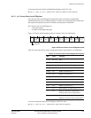
Table 4-24 Auxiliary Control Register bit functions (continued)
Bits Field Function