


Cycle Timings and Interlock Behavior
ARM DDI 0363E Copyright © 2009 ARM Limited. All rights reserved. 14-20
ID013010 Non-Confidential, Unrestricted Access
14.12 Load and Store Double instructions
This section describes the cycle timing behavior for the
LDRD
and
STRD
instructions.
The
LDRD
and
STRD
instructions:
• Are normally single-cycle issue. Both the base and any offset register are Very Early Regs.
• Are 3-cycle issue if offset or pre-increment addressing with a negative register offset is
used. Both the base and any offset register are Very Early Regs.
• Take only one memory cycle if the address is doubleword aligned.
• Take two memory cycles if the address is not doubleword aligned.
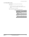
Table 14-15 shows the cycle timing behavior for
LDRD
and
STRD
instructions.
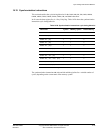
Table 14-16 shows the explanation of
<addr_md_1cycle>
and
<addr_md_3cycle>
used in
Table 14-15.
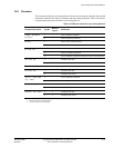
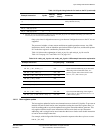
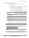
Table 14-15 Load and Store Double instructions cycle timing behavior
Example instruction Cycles
Cycles with
base writeback
Memory
cycles
Result
latency
(LDRD)
Result latency
(base register)
Address is doubleword aligned
LDRD R0, R1, <addr_md_1cycle>
a
12 1 2, 22
LDRD R0, R1, <addr_md_3cycle>
a
34 1 4, 44
Address not doubleword aligned
LDRD R0, R1, <addr_md_1cycle>
a
22 2 2, 32
LDRD R0, R1, <addr_md_3cycle>
a
44 2 4, 54
a. See Table 14-16 for an explanation of
<addr_md_1cycle>
and
<addr_md_3cycle>
.
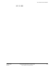
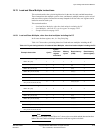
Table 14-16 <addr_md_1cycle> and <addr_md_3cycle> LDRD example instruction explanation
Example instruction Very Early Reg Comments
<addr_md_1cycle>
LDRD <Rt>, <Rt2>, [<Rn>, #<imm>] (!) <Rn>
If post-increment addressing, pre-increment
addressing with an immediate offset or a positive
register offset, then 1-issue cycle
LDRD <Rt>, <Rt2>, [<Rn>, <Rm>] (!) <Rn>, <Rm>
LDRD <Rt>, <Rt2>, [<Rn>], #<imm> <Rn>
LDRD <Rt>, <Rt2>, [<Rn>], +/-<Rm> <Rn>, <Rm>
<addr_md_3cycle>
LDRD <Rt>, <Rt2>, [<Rn>, -<Rm>] (!) <Rn>,<Rm>
If pre-increment addressing with a negative
register offset, then 3-issue cycles