


System Control Coprocessor
ARM DDI 0363E Copyright © 2009 ARM Limited. All rights reserved. 4-5
ID013010 Non-Confidential, Unrestricted Access
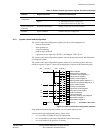
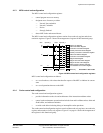
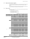
4.1.3 MPU control and configuration
The MPU control and configuration registers:
• control program access to memory
• designate areas of memory as either:
— Normal, Non-cacheable
— Normal, Cacheable
—Device
— Strongly Ordered.
• detect MPU faults and external aborts.
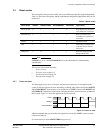
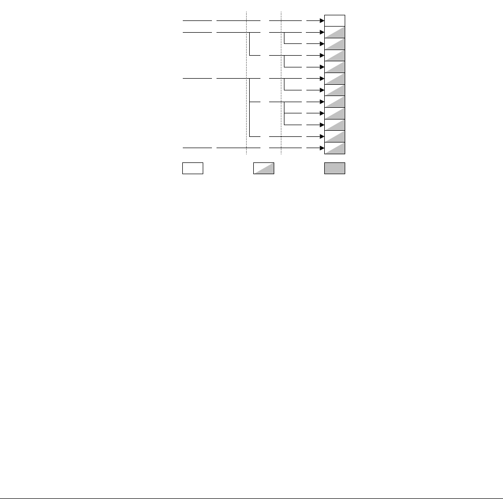
The MPU control and configuration registers consist of one read-only register and eleven
read/write registers. Figure 4-2 shows the arrangement of registers in this functional group.
Figure 4-2 MPU control and configuration registers
MPU control and configuration can behave:
• as a set of numbers, with values that describe aspects of the MPU or indicate its current
state
• as a set of operations that act on the MPU.
4.1.4 Cache control and configuration
The cache control and configuration registers:
• provide information on the size and architecture of the instruction and data caches
• control cache maintenance operations that include clean and invalidate caches, drain and
flush buffers, and address translation
• override cache behavior during debug or interruptible cache operations.
The cache control and configuration registers consist of three read-only registers, one read/write
register, and a number of write-only registers. Figure 4-3 on page 4-6 shows the arrangement of
the registers in this functional group.
4
MPU Type Registerc00
Opcode_2CRmCRn Opcode_1
1
Data Fault Address Register
Data Fault Status Register
0
0
c5
Region Size and Enable Register
Region Base Register
Region Access Control Register
Memory Region Number Register
Instruction Fault Address Register
Instruction Fault Status Register
1
Auxilary Data Fault Status Register
Auxilary Instruction Fault Status Register
0
c0
0 c0
c1
c6
0 c0
0
c1
2
4
0
c2
2
Write-only
Accessible in User mode
Read-only Read/write
0
Correctable Fault Location Registerc15
c30