


Cycle Timings and Interlock Behavior
ARM DDI 0363E Copyright © 2009 ARM Limited. All rights reserved. 14-25
ID013010 Non-Confidential, Unrestricted Access
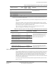
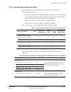
14.15 Synchronization instructions
This section describes the cycle timing behavior for the
CLREX
,
DMB
,
DSB
,
ISB
,
LDREX
,
LDREXB
,
LDREXD
,
LDREXH
,
STREX
,
STREXB
,
STREXD
,
STREXH
,
SWP
, and
SWPB
instructions
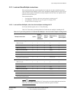
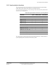
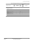
In all cases the base register, Rn, is a Very Early Reg. Table 14-20 shows the synchronization
instructions cycle timing behavior.
The synchronization instructions
DMB
,
DSB
, and
ISB
stall the pipeline for a variable number of
cycles, depending on the current state of the memory system.
Table 14-20 Synchronization instructions cycle timing behavior
Instruction Cycles Memory cycles Result latency
CLREX
1- -
LDREX <Rt>, [Rn]
11 2
LDREXB <Rt>, [Rn]
11 2
LDREXH <Rt>, [Rn]
11 2
LDREXD <Rt>, [Rn]
a
a. Address must be 64-bit aligned.
11 2
STREX <Rd>, <Rt>, [Rn]
11 2
STREXB <Rd>, <Rt>, [Rn]
11 2
STREXH <Rd>, <Rt>, [Rn]
11 2
STREXD <Rd>, <Rt>, <Rt2>, [Rn]
a
11 2
SWP <Rt>, <Rt2>, [Rn]
22 3
SWPB <Rt>, <Rt2>, [Rn]
22 3