


Level Two Interface
ARM DDI 0363E Copyright © 2009 ARM Limited. All rights reserved. 9-26
ID013010 Non-Confidential, Unrestricted Access
• There is no TCM present. The mapping of bus addresses to ARUSERS and ARADDRS
is determined when the processor is integrated. You must understand this mapping to use
of the AXI-slave interface within your system.
9.6.2 Cache RAM access
This section contains the following:
• Memory map when accessing the cache RAMs
• Data RAM access on page 9-27
• Tag RAM access on page 9-29
• Dirty RAM access on page 9-31.
• Other examples of accessing cache RAMs on page 9-32
Memory map when accessing the cache RAMs
The memory maps for the data and instruction caches have the same format. Because the
instruction cache does not have a dirty RAM, accesses to it generate the SLVERR error
response.
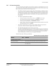
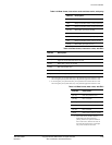
Table 9-29, Table 9-30, and Table 9-31 on page 9-27 show the chip-select decodes for selecting
the cache RAMs in the processor.
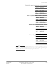
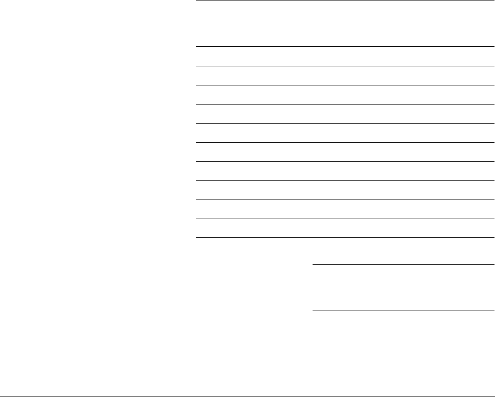
Table 9-29 Cache RAM chip-select decode
Inputs
RAM selected
ARUSERS[3:0] ARADDRS[22:19]
0100 0000 Instruction cache data RAM
0100 0001 Instruction cache tag RAM
0100 0010 Not used, generates an error
0100 0011 Not used, generates an error
0100 ARADDRS[22:21] != 00 Not used, generates an error
1000 0000 Data cache data RAM
1000 0001 Data cache tag RAM
1000 0010 Data cache dirty RAM
1000 0011 Not used, generates an error
1000 ARADDRS[22:21] != 00 Not used, generates an error
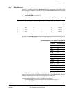
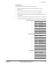
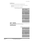
Table 9-30 Cache tag/valid RAM bank/address decode
Inputs
RAM bank
selected
Cache
way
ARADDRS[18:15]
0001 Bank 0 0