


AC Characteristics
ARM DDI 0363E Copyright © 2009 ARM Limited. All rights reserved. 15-8
ID013010 Non-Confidential, Unrestricted Access
The timing parameters for the dual-redundant core compare logic input control buses,
DCCMINP[7:0] and DCCMINP2[7:0], are implementation-defined. Contact the implementer
of the macrocell you are working with.
15.2.2 Output ports timing parameters
Most output ports have a maximum output delay of 60%, that is the SoC is enabled to use 60%
of the clock cycle.
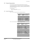
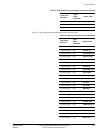
Table 15-10 shows the timing parameter for the miscellaneous output port.
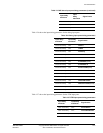
Table 15-11 shows the timing parameters for the interrupt output ports.
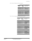
Table 15-12 shows the timing parameters for the AXI master output port.
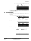
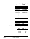
Clock uncertainty 50% B1TCWAIT
Clock uncertainty 40% B1TCLATEERROR
Clock uncertainty 50% B1TCRETRY
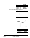
Table 15-9 TCM interface input ports timing parameters (continued)
Input delay
minimum
Input
delay
maximum
Signal name
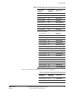
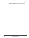
Table 15-10 Miscellaneous output port timing parameter
Output delay
minimum
Output delay
maximum
Signal name
Clock uncertainty 10% STANDBYWFI
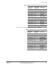
Table 15-11 Interrupt output ports timing parameters
Output delay
minimum
Output delay
maximum
Signal name
Clock uncertainty 60% IRQACK
Clock uncertainty 60% nPMUIRQ
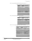
Table 15-12 AXI master output port timing parameters
Output delay
minimum
Output delay
maximum
Signal name
Clock uncertainty 60% AWIDM[3:0]
Clock uncertainty 60% AWADDRM[31:0]
Clock uncertainty 60% AWLENM[3:0]
Clock uncertainty 60% AWSIZEM[2:0]
Clock uncertainty 60% AWBURSTM[1:0]
Clock uncertainty 60% AWLOCKM[1:0]
Clock uncertainty 60% AWCACHEM[3:0]