Cycle Timings and Interlock Behavior
ARM DDI 0363E Copyright © 2009 ARM Limited. All rights reserved. 14-3
ID013010 Non-Confidential, Unrestricted Access
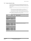
14.1 About cycle timings and interlock behavior
Complex instruction dependencies and memory system interactions make it impossible to
describe briefly the exact cycle timing behavior for all instructions in all circumstances. The
timings described in this chapter are accurate in most cases. If precise timings are required, you
must use a cycle-accurate model of the processor.
Unless stated otherwise, cycle counts and result latencies that this chapter describes are
best-case numbers. They assume:
• no outstanding data dependencies between the current instruction and a previous
instruction
• the instruction does not encounter any resource conflicts
• all data accesses hit in the data cache, and do not cross protection region boundaries
• all instruction accesses hit in the instruction cache.
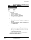
This section describes:
• Instruction execution overview
• Conditional instructions on page 14-4
• Flag-setting instructions on page 14-4
• Definition of terms on page 14-4.
• Assembler language syntax on page 14-5.
14.1.1 Instruction execution overview
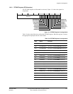
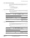
The instruction execution pipeline has four stages, Iss, Ex1, Ex2, and Wr.
Extensive forwarding to the end of the Iss, Ex1, and Ex2 stages enables many dependent
instruction sequences to run without pipeline stalls. General forwarding occurs from the end of
the Ex2 and Wr pipeline stages. In addition, the multiplier contains an internal multiply
accumulate forwarding path. The address generation unit also contains an internal forwarding
path.
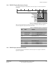
Most instructions do not require a register until the Ex2 stage. All result latencies are given as
the number of cycles until the register is available for a following instruction in the Ex2 stage.
Most ALU operations require their source registers at the start of the Ex2 stage, and have a result
latency of one. For example, the following sequence takes two cycles:
ADD R1,R3,R4 ;Result latency one
ADD R5,R2,R1 ;Register R1 required by ALU
The PC is the only register that result latency does not affect. An instruction that alters the PC
never causes a pipeline stall because of interlocking with a subsequent instruction that reads the
PC.
Most loads have a result latency of two or higher as they do not forward their results until the
Wr stage. For example, the following sequence takes three cycles:
LDR R1, [R2] ;Result latency two
ADD R3, R3, R1 ;Register R1 required by ALU
If a subsequent instruction requires the register at the end of the Iss stage then an extra cycle
must be added to the result latency of the instruction producing the required register.
Instructions that require a register at the end of these stages are specified by describing that
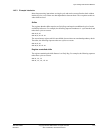
register as an Early Reg. The following sequence, requiring an Early Reg, takes four cycles:
LDR R1, [R2] ;Result latency two


