


Cycle Timings and Interlock Behavior
ARM DDI 0363E Copyright © 2009 ARM Limited. All rights reserved. 14-24
ID013010 Non-Confidential, Unrestricted Access
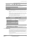
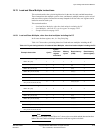
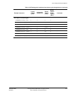
14.14 RFE and SRS instructions
This section describes the cycle timing for the
RFE
and
SRS
instructions.
These instructions:
• return from an exception and save exception return state respectively
• take one or two memory cycles depending on doubleword alignment first address
location.
In all cases the base register is a Very Early Reg.
Table 14-19 shows the cycle timing behavior for
RFE
and
SRS
instructions.
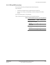
Table 14-19 RFE and SRS instructions cycle timing behavior
Example instruction Cycles Memory cycles
Address doubleword aligned
RFEIA <Rn>
10 1
SRSIA #<mode>
11
Address not doubleword aligned
RFEIA <Rn>
11 2
SRSIA #<mode>
22