


Level One Memory System
ARM DDI 0363E Copyright © 2009 ARM Limited. All rights reserved. 8-30
ID013010 Non-Confidential, Unrestricted Access
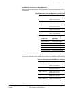
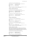
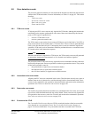
Table 8-13 shows the organization of the data cache RAM bits when parity is implemented.
Parity bits are grouped together in bits[35:32] so that data and parity bits are easily
differentiated. With this design the parity bit is selected alongside the related data byte, so that
when data is updated, the parity bit is also updated.
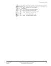
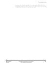
Data RAM sizes with ECC implemented
Table 8-14 shows the organization for the instruction cache when ECC is implemented. For
ECC error detection, eight bits are added per 64 bits, so four bits are added for each RAM bank.
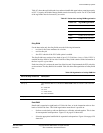
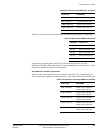
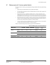
Table 8-12 Data cache data RAM sizes, with parity
Cache size Data RAMs
4KB, 4 1KB ways 8 banks 36 bits 128 lines
8KB, 4 2KB ways 8 banks 36 bits 256 lines
16KB, 4 4KB ways 8 banks 36 bits 512 lines
32KB, 4 8KB ways 8 banks 36 bits 1024 lines
64KB, 4 16KB ways 8 banks 36 bits 2048 lines
Table 8-13 Data cache RAM bits, with parity
RAM bits Description
Bit [35] Parity bit for byte[31:24]
Bit [34] Parity bit for byte[23:16]
Bit [33] Parity bit for byte[15:8]
Bit [32] Parity bit for byte[7:0]
Bits [31:0] Data[31:0]
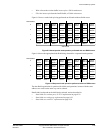
Table 8-14 Instruction cache data RAM sizes with ECC
Cache size Data RAMs
4KB, 4 1KB ways 4 banks 72 bits 128 lines or
8 banks 36 bits 128 lines
8KB, 4 2KB ways 4 banks 72 bits 256 lines or
8 banks 36 bits 256 lines
16KB, 4 4KB ways 4 banks 72 bits 512 lines or
8 banks 36 bits 512 lines
32KB, 4 8KB ways 4 banks 72 bits 1024 lines or
8 banks 36 bits 1024 lines
64KB, 4 16KB ways 4 banks 72 bits 2048 lines or
8 banks 36 bits 2048 lines