


System Control Coprocessor
ARM DDI 0363E Copyright © 2009 ARM Limited. All rights reserved. 4-44
ID013010 Non-Confidential, Unrestricted Access
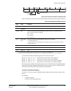
To access the Secondary Auxiliary Control Register, read or write CP15 with:
MRC p15, 0, <Rd>, c15, c0, 0 ; Read Secondary Auxiliary Control Register
MCR p15, 0, <Rd>, c15, c0, 0 ; Write Secondary Auxiliary Control Register
ARM recommends that any instruction that changes bits [20:16] is followed by an
ISB
instruction to ensure that the changes have taken effect before any dependent instructions are
executed.
4.2.17 c1, Coprocessor Access Register
The Coprocessor Access Register sets access rights for coprocessors CP0-CP13. This register
has no effect on access to CP14, the debug control coprocessor, or CP15, the system control
coprocessor. This register also provides a means for software to determine if any particular
coprocessor, CP0-CP13, exists in the system.
The Coprocessor Access Register is:
• a read/write register
• accessible in Privileged mode only.
Because this processor does not support coprocessors CP0 through CP9, CP12, and CP13, bits
[27:24] and [19:0] in this register are read-as-zero and ignore writes.
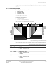
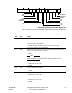
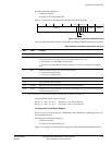
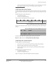
Figure 4-30 shows the arrangement of bits in the register.
Figure 4-30 Coprocessor Access Register format
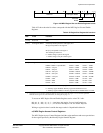
[2] ATCMECC
Correction for internal ECC logic on ATCM port.
d
0 = Enabled. This is the reset value.
1 = Disabled.
[1] BTCMRMW Enables 64-bit stores for the BTCMs. When enabled, the processor uses read-modify-write to
ensure that all reads and writes presented on the BTCM ports are 64 bits wide.
e
0 = Disabled
1 = Enabled.
The primary input RMWENRAM[1] defines the reset value.
[0] ATCMRMW Enables 64-bit stores for the ATCM. When enabled, the processor uses read-modify-write to
ensure that all reads and writes presented on the ATCM port are 64 bits wide.
e
0 = Disabled
1 = Enabled.
The primary input RMWENRAM[0] defines the reset value.
a. This bit is RAZ if both caches have neither ECC nor parity.
b. This bit is only supported if parity error generation is implemented in your design.
c. This bit has no effect unless the Floating Point Unit (FPU) has been configured, see Configurable options on page 1-13.
d. This bit has no effect unless TCM ECC logic has been configured for the respective TCM interface, see Configurable options
on page 1-13.
e. This feature is not available when the TCM interface has been built with 32-bit ECC.
Table 4-25 Secondary Auxiliary Control Register bit functions (continued)
Bits Field Function
Reserved
31 28 27 26 25 24 23
22
21
20 19 18
17
16 15 14 13 12 11 10 9 8 7 6 5 4 3 2 1 0
cp13 cp12 cp11 cp10 cp9 cp8 cp7 cp6 cp5 cp4 cp3 cp2 cp1 cp0