Processor Signal Descriptions
ARM DDI 0363E Copyright © 2009 ARM Limited. All rights reserved. A-9
ID013010 Non-Confidential, Unrestricted Access
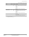
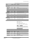
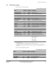
AW VA LIDM Output CLKIN Indicates address and control are valid.
Write data channel
WDATAM[63:0] Output CLKIN Write data.
WIDM[3:0] Output CLKIN The identification tag for the write data group of signals.
WLASTM Output CLKIN Indicates the last data transfer of a burst.
WREADYM Input CLKIN Indicates that the slave is ready to accept write data
WSTRBM[7:0] Output CLKIN Write strobes used to indicate which byte lanes must be updated.
WVALIDM Output CLKIN Indicates address and control are valid.
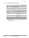
Write response channel
BIDM [3:0] Input CLKIN The identification tag for the write response signal.
BREADYM Output CLKIN Indicates that the core is ready to accept write response.
BRESPM[1:0] Input CLKIN Write response.
BVALIDM Input CLKIN Indicates that a valid write response is available.
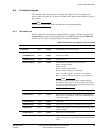
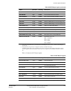
Read address channel
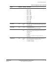
ARADDRM[31:0] Output CLKIN Instruction fetch burst start address.
ARBURSTM[1:0] Output CLKIN Burst type.
ARCACHEM[3:0] Output CLKIN Provides decode information for outer attributes:
b0000 = Strongly Ordered.
b0001 = Device.
b0011 = Normal, Non-cacheable.
b0110 = Normal, Cacheable. write-through.
b1111 = Normal, Cacheable. write-back, write allocation.
b0111 = Normal, Cacheable. write-back, no write allocation.
Note
The AXI specification describes these encodings using the
pre-ARMv6 terms such as cacheable-bufferable. These terms
are equivalent to the ARMv6 memory-type descriptions such as
Normal, Non-cacheable used here.
ARIDM[3:0] Output CLKIN Identification tag for the read address group of signals
ARLENM [3:0] Output CLKIN Instruction fetch burst length.
ARLOCKM[1:0] Output CLKIN Lock signal.
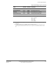
ARPROTM[2:0] Output CLKIN Protection signals provide addition information about a bus
access.
ARREADYM Input CLKIN Address ready. The slave uses this signal to indicate that it can
accept the address.
ARSIZEM[2:0] Output CLKIN Indicates the size of the transfer.
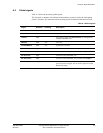
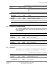
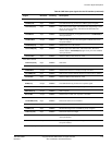
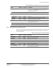
Table A-4 AXI master port signals for the L2 interface (continued)
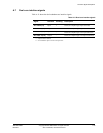
Signal Direction Clocking Description


