


CHAPTER 6 PERIPHERAL HARDWARE FUNCTION
101
User’s Manual U10676EJ3V0UM
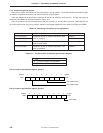
6.1.6 I/O timing of digital I/O port
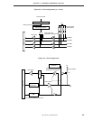
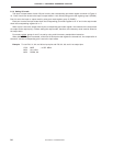
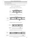
Figure 6-12 shows the timing at which data is output to the output latch and the timing at which the pin data or
the data of the output latch is loaded to the internal bus.
Figure 6-13 shows the ON timing when an on-chip pull-up resistor connection is specified via software.
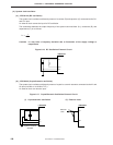
Figure 6-12. I/O Timing of Digital I/O Port
(a) When data is loaded by 1-machine-cycle instruction
Instruction
execution
Manipulation
instruction
1 machine cycle
Input timing
Φ0 Φ1 Φ2 Φ3
(b) When data is loaded by 2-machine-cycle instruction
Instruction
execution
Input timing
2 machine cycles
Manipulation instruction
Φ
0
Φ
1
Φ
2
Φ
3
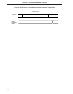
(c) When data is latched by 1-machine-cycle instruction
Instruction
execution
Manipulation
instruction
Φ
3
Φ
0
Φ
1
Output latch
(output pin)
(d) When data is latched by 2-machine-cycle instruction
Instruction
execution
Φ
0
Φ
1
Output latch
(output pin)
Manipulation instruction