


CHAPTER 6 PERIPHERAL HARDWARE FUNCTION
96 User’s Manual U10676EJ3V0UM
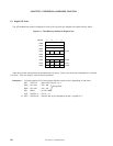
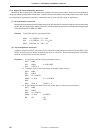
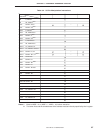
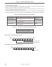
6.1.3 Digital I/O port manipulation instruction
Because all the I/O ports of the
µ
PD754244 are mapped to the data memory space, they can be manipulated by
using data memory manipulation instructions. Table 6-2 shows these data memory manipulation instructions, which
are considered to be especially useful for manipulating the I/O pins and their range of applications.
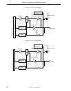
(1) Bit manipulation instruction
Because specific address bit direct addressing (fmem.bit) and specific address bit register indirect addressing
(pmem.@L) are applicable to digital I/O ports 3, 6, and 8, the bits of these ports can be manipulated regardless
of the specifications by MBE and MBS.
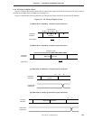
Example To OR P30 and P61 and output to P80
MOV1 CY, PORT3.0 ; CY ← P30
OR1 CY, PORT6.1 ; CY ← CY P61
MOV1 PORT8.0, CY ; P80 ← CY
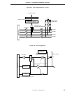
(2) 4-bit manipulation instruction
In addition to the IN and OUT instructions, all the 4-bit memory manipulation instructions such as MOV, XCH,
ADDS, and INCS can be used to manipulate the ports in 4-bit units. Before executing these instructions,
however, memory bank 15 must be selected.
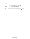
Examples 1. To output the contents of the accumulator to port 3
SET1 MBE
SEL MB15 ; or CLR1 MBE
OUT PORT3, A
2. To add the value of the accumulator to the data output to port 6
SET1 MBE
SEL MB15
MOV HL, #PORT6
ADDS A, @HL ; A ← A+PORT6
NOP
MOV @HL, A ; PORT6 ← A
3. To test whether the data of port 3 is greater than the value of the accumulator
SET1 MBE
SEL MB15
MOV HL, #PORT3
SUBS A, @HL ; A<PORT3
BR NO ; NO
; YES