


CHAPTER 6 PERIPHERAL HARDWARE FUNCTION
109
User’s Manual U10676EJ3V0UM
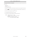
Cautions 1. The X2 pin of the
µ
PD754244 is internally pulled up to VDD by a resistor of 50 kΩ (typ.)
in the STOP mode.
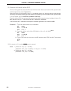
2. Wire the portion enclosed by the dotted lines in Figures 6-16 and 6-17 as follows to
prevent adverse influence by wiring capacitance when using the system clock oscil-
lator.
• Keep the wiring length as short as possible.
• Do not cross the wiring with any other signal lines.
• Do not route the wiring in the vicinity of a line through which a high alternating
current is flowing.
• Always make the potential at the connecting point of the capacitor of the oscillator
the same level as V
SS.
Do not connect the wiring to a ground pattern through which a high current is
flowing.
• Do not fetch signals from the oscillator.
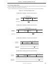
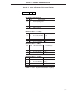
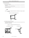
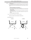
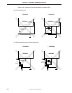
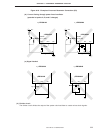
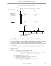
Figure 6-18 shows incorrect examples of connecting the resonator.
Figure 6-18. Example of Incorrect Resonator Connection (1/3)
(a) Wiring length too long
µ
PD754144
CL1 CL2 VSS
µ
PD754244
X1 X2 VSS
µ
• PD754144
µ
• PD754244