


14 User’s Manual U10676EJ3V0UM
LIST OF FIGURES (2/3)
Figure No. Title Page
6-18 Example of Incorrect Resonator Connection ..................................................................................... 109
6-19 CPU Clock Switching Example .......................................................................................................... 113
6-20 Block Diagram of Basic Interval Timer/Watchdog Timer ................................................................... 114
6-21 Format of Basic Interval Timer Mode Register .................................................................................. 116
6-22 Format of Watchdog Timer Enable Flag (WDTM) ............................................................................. 117
6-23 Block Diagram of Timer Counter (Channel 0) ................................................................................... 123
6-24 Block Diagram of Timer Counter (Channel 1) ................................................................................... 124
6-25 Block Diagram of Timer Counter (Channel 2) ................................................................................... 125
6-26 Format of Timer Counter Mode Register (Channel 0) ...................................................................... 127
6-27 Format of Timer Counter Mode Register (Channel 1) ...................................................................... 128
6-28 Format of Timer Counter Mode Register (Channel 2) ...................................................................... 130
6-29 Format of Timer Counter Output Enable Flag ................................................................................... 132
6-30 Format of Timer Counter Control Register ........................................................................................ 133
6-31 Setting of Timer Counter Mode Register ........................................................................................... 135
6-32 Setting of Timer Counter Control Register ........................................................................................ 138
6-33 Setting of Timer Counter Output Enable Flag ................................................................................... 138
6-34 Configuration When Timer Counter Operates ................................................................................... 143
6-35 Count Operation Timing ...................................................................................................................... 143
6-36 Setting of Timer Counter Mode Register ........................................................................................... 146
6-37 Setting of Timer Counter Control Register ........................................................................................ 147
6-38 PWM Pulse Generator Operating Configuration ............................................................................... 149
6-39 PWM Pulse Generator Operating Timing .......................................................................................... 149
6-40 Setting of Timer Counter Mode Registers ......................................................................................... 152
6-41 Setting of Timer Counter Control Register ........................................................................................ 153
6-42 Configuration When Timer Counter Operates ................................................................................... 157
6-43 Timing of Count Operation ................................................................................................................. 158
6-44 Setting of Timer Counter Mode Register (n = 1, 2) ........................................................................... 161
6-45 Setting of Timer Counter Output Enable Flag ................................................................................... 162
6-46 Setting of Timer Counter Control Register ........................................................................................ 162
6-47 Configuration in Carrier Generator Mode .......................................................................................... 165
6-48 Carrier Generator Operation Timing .................................................................................................. 166
6-49 Block Diagram of Programmable Threshold Port .............................................................................. 181
6-50 Format of Programmable Threshold Port Mode (PTHM) Register ................................................... 182
6-51 Application Example of Programmable Threshold Port..................................................................... 183
6-52 Format of Bit Sequential Buffer .......................................................................................................... 184
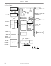
7-1 Block Diagram of Interrupt Controller ................................................................................................ 187
7-2 Interrupt Vector Table .......................................................................................................................... 189
7-3 Interrupt Priority Select Register ........................................................................................................ 192
7-4 Configuration of INT0.......................................................................................................................... 194
7-5 I/O Timing of Noise Eliminator ........................................................................................................... 194
7-6 Format of INT0 Edge Detection Mode Register (IM0) ...................................................................... 195
7-7 Interrupt Servicing Sequence ............................................................................................................. 197
7-8 Nesting of Interrupt with High Priority ................................................................................................ 198