


CHAPTER 6 PERIPHERAL HARDWARE FUNCTION
124 User’s Manual U10676EJ3V0UM
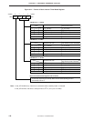
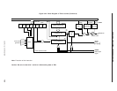
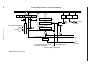
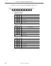
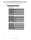
Figure 6-24. Block Diagram of Timer Counter (Channel 1)
Note Execution of the instruction
8
Internal bus
TM16– TM15 TM14 TM13 TM12 TM11 TM10
TM1
Timer counter (channel 2) output
From clock
generator
MPX
Decoder
8
Modulo register (8)
8
TMOD1
Comparator (8)
8
Count register (8)
T1
CP
Clear
Reset
IRQT1 clear
signal
RESET
Selector
INT1
lRQT1
set signal
Timer counter (channel 2) comparator
(in 16-bit timer counter mode)
Timer counter (channel 2) match signal
(in 16-bit timer counter mode)
Timer counter (channel 2)
reload signal
T1 enable
flag
TOE1
P31
output latch
PORT3.1
Port 2
l/O mode
Bit 1 of PMGA
P31/PTO1
Output buffer
Co-
inci-
dence
Timer operation starts
16-bit timer counter mode
TOUT
F/F
fX/2
5
fX/2
6
fX/2
8
fX/2
10
fX/2
12
SET1
Note