


CHAPTER 4 INTERNAL CPU FUNCTION
69
User’s Manual U10676EJ3V0UM
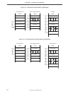
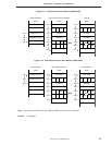
03
B
03
C
03
D
03
E
03
H
03
L
03
X
03
A
One bank
000H
001H
002H
003H
004H
005H
006H
007H
008H
00FH
010H
017H
018H
.
.
.
.
.
01FH
Same configura-
tion as bank 0
Same configura-
tion as bank 0
Same configura-
tion as bank 0
Register bank 0
Register bank 1
Register bank 2
Register bank 3
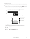
03
Address Data memory
A register
X register
L register
H register
E register
D register
C register
B register
.
.
.
.
.
.
.
.
.
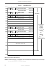
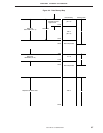
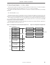
4.5 General-Purpose Registers ... 8 × 4 bits × 4 banks
General-purpose registers are mapped to the specific addresses of the data memory. Four banks of registers,
with each bank consisting of eight 4-bit registers (B, C, D, E, H, L, X, and A), are available.
The register bank (RB) that becomes valid when an instruction is executed is determined by the following
expression.
RB = RBE
RBS (RBS = 0 to 3)
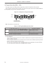
Each general-purpose register is manipulated in 4-bit units. Moreover, two registers can be used in pairs, such
as BC, DE, HL, and XA, and manipulated in 8-bit units. Register pairs DE, HL, and DL are also used as data pointers.
When registers are manipulated in 8-bit units, the register pairs of the register bank (RB) with bit 0 inverted (0
↔ 1, 2 ↔ 3), BC’, DE’, HL’, and XA’, can also be used in addition to BC, DE, HL, and XA (refer to 3.2 Bank
Configuration of General-Purpose Registers).
The general-purpose register area can be addressed and accessed as an ordinary RAM area, regardless of
whether the registers in this area are used or not.
Figure 4-5. Configuration of General-Purpose Register Area Figure 4-6. Configuration of Register Pair
.