


CHAPTER 7 INTERRUPT AND TEST FUNCTIONS
193
User’s Manual U10676EJ3V0UM
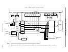
(3) Hardware of INT0
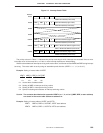
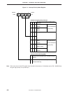
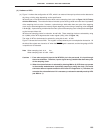
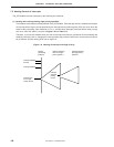
(a) Figure 7-4 shows the configuration of INT0, which is an external interrupt input that can be detected at
the rising or falling edge depending on the specification.
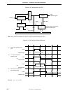
INT0 also has a noise elimination function which uses a sampling clock (refer to Figure 7-5 I/O Timing
of Noise Eliminator). The noise eliminator eliminates a pulse having a width narrower than 2 cycles
Note
of the sampling clock as noise. However, a pulse having a width wider than one cycle of the sampling
clock may be acknowledged as the interrupt signal depending on the timing of sampling (refer to Figure
7-5 <2> (a)). A pulse having a width wider than two cycles of the sampling clock is always acknowledged
as the interrupt without fail.
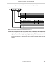
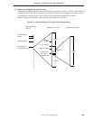
INT0 has two sampling clocks for selection: Φ and f
X/64. These sampling clocks are selected by using
bit 3 (IM03) of the INT0 edge detection mode register (IM0) (refer to Figure 7-6).
The edge of INT0 to be detected is selected by using bits 0 and 1 of IM0.
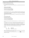
Figure 7-6 shows the format of IM0. This register is manipulated by a 4-bit manipulation instruction. All
the bits of this register are cleared to “0” when the RESET signal is asserted, and the rising edge of INT0
is specified to be detected.
Note When sampling clock is Φ:2t
CY
When sampling clock is fX/64: 128/fX
Cautions 1. Even when a signal is input to the INT0/P61 pin in the port mode, it is input through
the noise eliminator. Therefore, input a signal having a width wider than two cycles
of the sampling clock.
2. When the noise eliminator is selected (by clearing IM02 to 0), INT0 does not operate
in the standby mode because it performs sampling by using the clock. (The noise
eliminator does not operate unless the CPU clock
Φ is supplied to it.) Therefore, do
not select the noise eliminator if it is necessary to release the standby mode by INT0
(set IM02 to 1).