


16 User’s Manual U10676EJ3V0UM
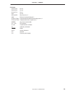
LIST OF TABLES
Table No. Title Page
2-1 Pin Functions of Digital I/O Ports ....................................................................................................... 24
2-2 Functions of Non-Port Pins ................................................................................................................ 25
2-3 Recommended Connection of Unused Pins ...................................................................................... 31
3-1 Addressing Modes .............................................................................................................................. 36
3-2 Register Bank Selected by RBE and RBS ........................................................................................ 45
3-3 Example of Using Different Register Banks for Normal Routine and Interrupt Routine .................. 45
3-4 Addressing Modes Applicable to Peripheral Hardware Unit Manipulation ....................................... 50
4-1 Differences Between MkI and MkII Modes ........................................................................................ 60
4-2 Stack Area Selected by SBS .............................................................................................................. 70
4-3 PSW Flags Saved/Restored to/from Stack ........................................................................................ 74
4-4 Carry Flag Manipulation Instruction ................................................................................................... 75
4-5 Contents of Interrupt Status Flags ..................................................................................................... 76
4-6 MBE, MBS, and Memory Bank Selected ........................................................................................... 78
4-7 RBE, RBS, and Register Bank Selected ........................................................................................... 79
5-1 Interrupt Related to EEPROM Control ............................................................................................... 82
6-1 Types and Features of Digital Ports ................................................................................................... 89
6-2 I/O Pin Manipulation Instructions ....................................................................................................... 97
6-3 Operation When I/O Port Is Manipulated ........................................................................................... 99
6-4 Specifying Connection of Pull-up Resistor ........................................................................................ 100
6-5 Maximum Time Required for CPU Clock Switching .......................................................................... 112
6-6 Mode List ............................................................................................................................................. 122
6-7 Resolution and Longest Set Time (8-Bit Timer Counter Mode)........................................................ 139
6-8 Resolution and Longest Set Time (16-Bit Timer Counter Mode)...................................................... 154
7-1 Types of Interrupt Sources ................................................................................................................. 188
7-2 Signals Setting Interrupt Request Flags ............................................................................................ 191
7-3 IST1 and IST0 and Interrupt Servicing Status .................................................................................. 196
7-4 Identifying Interrupt Sharing Vector Address ..................................................................................... 200
7-5 Types of Test Sources ......................................................................................................................... 212
7-6 Test Request Flag Setting Signals ..................................................................................................... 212
7-7 KR4 to KR7 Pins, KRREN Pin and Test Function ............................................................................. 214
8-1 Operating Statuses in Standby Mode ................................................................................................ 216
8-2 Selecting Wait Time by BTM .............................................................................................................. 220
9-1 Status of Each Hardware Unit After Reset ........................................................................................ 229
9-2 WDF and KRF Contents Corresponding to Each Signal .................................................................. 231
10-1 Selection of Mask Options .................................................................................................................. 233
11-1 Types of Bit Manipulation Addressing Modes and Specification Range .......................................... 235