


CHAPTER 4 INTERNAL CPU FUNCTION
65
User’s Manual U10676EJ3V0UM
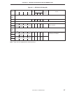
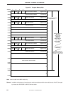
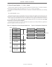
4.4 Data Memory (RAM) ... 128 words × 4 bits
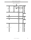
The data memory consists of data areas and a peripheral hardware area as shown in Figure 4-4.
The data memory consists the following banks with each bank made up of 256 words × 4 bits.
• Memory bank 0 (data areas)
• Memory bank 4 (EEPROM)
• Memory bank 15 (peripheral hardware area)
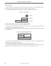
4.4.1 Configuration of data memory
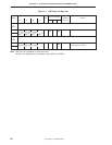
(1) Data area
A data area consists of a static RAM and is used to store data, and as a stack memory when a subroutine
or interrupt is executed. The contents of this area can be retained for a long time by battery backup even
when the CPU is halted in standby mode. The data area is manipulated by using memory manipulation
instructions.
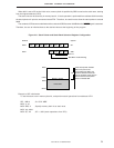
Static RAM is mapped to memory bank 0 in units of 128 words × 4 bits only. Although bank 0 is mapped as
a data area, it can also be used as a general-purpose register area (000H to 01FH) and as a stack area (000H
to 07FH).
One address of the static RAM consists of 4 bits. However, it can be manipulated in 8-bit units by using an
8-bit memory manipulation instruction or in 1-bit units by using a bit manipulation instruction. To use an 8-
bit manipulation instruction, specify an even address.
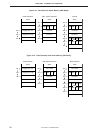
• General-purpose register area
This area can be manipulated by using a general-purpose register manipulation instruction or memory
manipulation instruction. Up to eight 4-bit registers can be used. The registers not used by the program
can be used as part of the data area or stack area.
• Stack area
The stack area is set by an instruction and is used as a saving area when a subroutine or interrupt service
is executed.
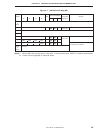
(2) EEPROM (Electrically Erasable PROM)
In EEPROM memory bank 4 (400H to 4FFH), only 16 words × 8 bits at 400H to 41FH are mapped.
Reading/writing of EEPROM is performed in 8-bit units.
Since 420H to 4FFH of memory bank 4 is an unmounted area, any value written to this area is ignored and
the read value becomes undefined.
(3) Peripheral hardware area
The peripheral hardware area is mapped to addresses F80H to FFFH of memory bank 15.
This area is manipulated by using a memory manipulation instruction, in the same manner as the static RAM.
Note, however, that the bit units in which the peripheral hardware units can be manipulated differ depending
on the address. The addresses to which no peripheral hardware unit is allocated cannot be accessed because
these addresses are not provided to the data memory.