


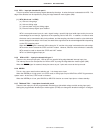

CHAPTER 3 FEATURES OF ARCHITECTURE AND MEMORY MAP
35
User’s Manual U10676EJ3V0UM
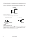
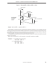
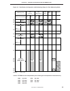
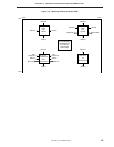
Figure 3-2. Data Memory Configuration and Addressing Range for Each Addressing Mode
000H
01FH
020H
07FH
0FFH
400H
41FH
4FFH
F80H
FB0H
FBFH
FC0H
FF0H
FFFH
General-
purpose
register area
Data area (SRAM)
Data area
(EEPROM16 × 8)
Memory bank 4
Peripheral
hardware area
(memory bank 15)
Not
incorporated
Not
incorporated
Addressing mode
mem
mem. bit
@HL
@H+mem. bit
@DE
@DL
Stack
addressing
fmem. bit
pmem. @L
Memory bank enable flag MBE = 0 MBE = 1 MBE = 0 MBE = 1 ––––
MBS =
15
MBS =
15
MBS = 4 MBS = 4
MBS = 0 MBS = 0 SBS = 0
Memory bank 0
Remark – : don’t care
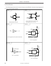
Caution EEPROM can be manipulated by the following 8-bit manipulation instructions only.
MOV XA, @HL XCH XA, @HL
MOV XA, mem XCH XA, mem
MOV @HL, XA SKE XA, @HL
MOV mem, XA