


CHAPTER 4 INTERNAL CPU FUNCTION
78 User’s Manual U10676EJ3V0UM
4.9 Bank Select Register (BS)
The bank select register (BS) consists of a register bank select register (RBS) and a memory bank select register
(MBS) which specify the register bank and the memory bank to be used, respectively.
RBS and MBS are set by the SEL RBn and SEL MBn instructions, respectively.
BS can be saved to or restored from the stack area in 8-bit units by the PUSH BS or POP BS instruction.
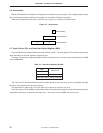
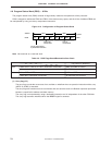
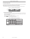
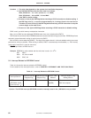
Figure 4-14. Configuration of Bank Select Register
RBS0RBS100MBS0MBS1MBS2MBS3
F82HF83H
Symbol
BS
Address
F82H
(1) Memory bank select register (MBS)
The memory bank select register is a 4-bit register that records the higher 4 bits of a 12-bit data memory
address. This register specifies the memory bank to be accessed. With the
µ
PD754244, however, only banks
0, 4 and 15 can be specified.
MBS is set by the SEL MBn instruction (n = 0, 4, 15).
The address range specified by MBE and MBS is as shown in Figure 3-2.
When the RESET signal is asserted, MBS is initialized to “0”.
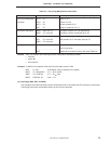
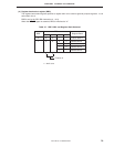
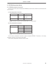
Table 4-6. MBE, MBS, and Memory Bank Selected
MBE MBS Memory Bank
3210
0 ××××Fixed to memory bank 0
1 0000Selects memory bank 0
0100Selects memory bank 4
1111Selects memory bank 15
Other than above Setting prohibited
× = don’t care