


13
User’s Manual U10676EJ3V0UM
LIST OF FIGURES (1/3)
Figure No. Title Page
3-1 Selecting MBE = 0 Mode and MBE = 1 Mode .................................................................................. 33
3-2 Data Memory Configuration and Addressing Range for Each Addressing Mode............................ 35
3-3 Updating Address of Static RAM ....................................................................................................... 39
3-4 Example of Using Register Banks ..................................................................................................... 46
3-5 Configuration of General-Purpose Registers (4-Bit Processing) ...................................................... 48
3-6 Configuration of General-Purpose Registers (8-Bit Processing) ...................................................... 49
3-7
µ
PD754244 I/O Map ........................................................................................................................... 52
4-1 Format of Stack Bank Select Register ............................................................................................... 61
4-2 Configuration of Program Counter ..................................................................................................... 62
4-3 Program Memory Map ........................................................................................................................ 64
4-4 Data Memory Map .............................................................................................................................. 67
4-5 Configuration of General-Purpose Register Area ............................................................................. 69
4-6 Configuration of Register Pair ............................................................................................................ 69
4-7 Accumulator ........................................................................................................................................ 70
4-8 Stack Pointer and Stack Bank Selection Register Configuration ..................................................... 71
4-9 Data Saved to Stack Memory (MkI Mode) ......................................................................................... 72
4-10 Data Restored from Stack Memory (MkI Mode) ................................................................................ 72
4-11 Data Saved to Stack Memory (MkII Mode) ........................................................................................ 73
4-12 Data Restored from Stack Memory (MkII Mode) ............................................................................... 73
4-13 Configuration of Program Status Word .............................................................................................. 74
4-14 Configuration of Bank Select Register ............................................................................................... 78
5-1 Format of EEPROM Write Control Register ...................................................................................... 81
5-2 EEPROM Write Control Register in EEPROM Read Manipulation .................................................. 84
5-3 EEPROM Write Control Register in EEPROM Write Manipulation................................................... 85
6-1 Data Memory Address of Digital Ports .............................................................................................. 88
6-2 P3n Configuration (n = 0 to 2)............................................................................................................ 90
6-3 P33 Configuration ............................................................................................................................... 90
6-4 P60 Configuration ............................................................................................................................... 91
6-5 P61 Configuration ............................................................................................................................... 91
6-6 P62 Configuration ............................................................................................................................... 92
6-7 P63 Configuration ............................................................................................................................... 92
6-8 P7n Configuration (n = 0 to 3)............................................................................................................ 93
6-9 P80 Configuration ............................................................................................................................... 93
6-10 Format of Each Port Mode Register .................................................................................................. 95
6-11 Format of Pull-up Resistor Specification Register ............................................................................ 100
6-12 I/O Timing of Digital I/O Port .............................................................................................................. 101
6-13 ON Timing of Internal Pull-up Resistor Connected via Software ..................................................... 102
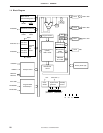
6-14 Block Diagram of Clock Generator ..................................................................................................... 103
6-15 Format of Processor Clock Control Register ..................................................................................... 107
6-16 RC Oscillation External Circuit ........................................................................................................... 108
6-17 Crystal/Ceramic Oscillation External Circuit ...................................................................................... 108