Appendix D Register Map and Descriptions
© National Instruments Corporation D-3 Lab-PC+ User Manual
Register Sizes
The Lab-PC+ registers are 8-bit registers. To transfer 16-bit data, two consecutive I/O readings
or writings are needed. For example, to read the 16-bit A/D conversion result, two consecutive
8-bit readings of FIFO are needed. The first reading returns the low byte of the 16-bit data, and
the second returns the high byte of the data.
Register Description
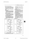
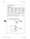
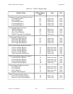
Table D-1 divides the Lab-PC+ registers into six different register groups. A bit description of
each of the registers making up these groups is included later in this chapter.
The Configuration and Status Register Group controls the overall operation of the Lab-PC+ and
the D/A circuitry. The Analog Input Register Group is used to read output from the 12-bit
successive-approximation ADC. The Analog Output Register Group accesses the two 12-bit
DACs. The two Counter/Timer Register Groups (A and B) access each of the two onboard 8253
Counter/Timer integrated circuits. The Digital I/O Register Group consists of the four registers
of the onboard 8255A PPI integrated circuit used for digital I/O. The Interval Counter registers
are used in the single-channel interval acquisition mode.
Register Description Format
The remainder of this register description chapter discusses each of the Lab-PC+ registers in the
order shown in Table D-1. Each register group is introduced, followed by a detailed bit
description of each register on the Lab-PC+. For a detailed bit description of each register
concerning the 8253 (A or B) chip on the Lab-PC+, refer to Appendix B, OKI 82C53 Data Sheet,
later in this manual. The individual register description gives the address, type, word size, and
bit map of the register, followed by a description of each bit.
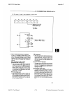
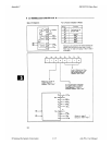
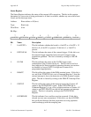
The register bit map shows a diagram of the register with the MSB (bit 7 for an 8-bit register)
shown on the left, and the LSB (bit 0) shown on the right. A square is used to represent each bit.
Each bit is labeled with a name inside its square. An asterisk (*) after the bit name indicates that
the bit is inverted (negative logic).
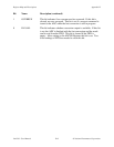
In many of the registers, several bits are labeled with an X, indicating don't care bits. When a
register is read, these bits may appear set or cleared but should be ignored because they have no
significance. When a register is written to, setting or clearing these bit locations has no effect on
the Lab-PC+ hardware.
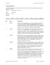
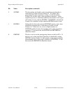
The bit map field for some write-only registers state not applicable, no bits used. Writing to
these registers causes some event to occur on the Lab-PC+, such as clearing the analog input
circuitry. The data is ignored when writing to these registers; therefore, any bit pattern will
suffice.


