Calibration Chapter 5
Lab-PC+ User Manual 5-6 © National Instruments Corporation
3. Gain Calibration
Adjust the analog input gain by applying an input voltage across ACH0 and
AISENSE/AIGND. This input voltage is +9.99634 V or V
+fs
- 1.5 LSB.
a. Connect the calibration voltage (+9.99634 V) across ACH0 (pin 1 on the I/O connector)
and AISENSE/AIGND (pin 9).
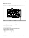
b. Take analog input readings from Channel 0 at a gain of 1, and adjust trimpot R5 until the
ADC readings flicker evenly between 4,094 and 4,095. Alternately, you can average a
number of readings (approximately 100) and adjust trimpot R10 until the average reading
is 4,094.5.
Analog Output Calibration
To null out error sources that affect the accuracy of the output voltages generated, you must
calibrate the analog output circuitry by adjusting the following potential sources of error:
• Analog output offset error
• Analog output gain error
Offset error in the analog output circuitry is the total of the voltage offsets contributed by each
component in the circuitry. This error appears as a voltage difference between the desired
voltage and the actual output voltage generated and is independent of the D/A setting. To correct
this offset gain error, set the D/A to negative full-scale and adjust a trimpot until the output
voltage is the negative full-scale value ±0.5 LSB.
Gain error in the analog output circuitry is the product of the gains contributed by each
component in the circuitry. This error appears as a voltage difference between the desired
voltage and the actual output voltage generated, which depends on the D/A setting. This gain
error is corrected by setting the D/A to positive full-scale and adjusting a trimpot until the output
voltage corresponds to the positive full-scale value ±0.5 LSB.
Board Configuration
The calibration procedure differs if you select either bipolar or unipolar output configuration. A
procedure for each configuration is given next.
Bipolar Output Calibration Procedure
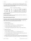
If your board is configured for bipolar output, which provides an output range of -5 to +5 V, then
complete the following procedures in the order given.


