


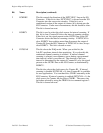

Register Map and Descriptions Appendix D
Lab-PC+ User Manual D-22 © National Instruments Corporation
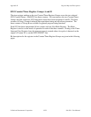
DAC0 Low-Byte (DAC0L), DAC0 High-Byte (DAC0H), DAC1 Low-Byte (DAC1L), and
DAC1 High-Byte (DAC1H) Registers
Writing to DAC0L and then to DAC0H loads the analog output Channel 0. Writing to DAC1L
and then to DAC1H loads the analog output Channel 1. The voltage generated by the analog
output channels is updated immediately after the corresponding DACxH register is written to, if
the corresponding LDACx bit is cleared in Command Register 2. If the LDACx bit is set, the
analog output is updated when an active low pulse occurs on the output of Counter A2 or on the
EXTUPDATE* line on the I/O connector.
Address: Base address + 04 (hex) Load DAC0 low byte.
Base address + 05 (hex) Load DAC0 high byte.
Base address + 06 (hex) Load DAC1 low byte.
Base address + 07 (hex) Load DAC1 high byte.
Type: Write-only (all)
Word Size: 8-bit (all)
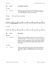
Bit Map:
DACxH
76543210
D15 D14 D13 D12 D11 D10 D9 D8
{ Sign Extension Bits }
DACxL
76543210
D7 D6 D5 D4 D3 D2 D1 D0
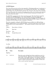
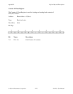
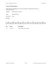
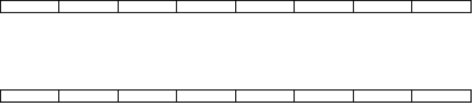
Bit Name Description
DACxH
7-4 D<15..12> Zero in straight binary mode, sign extension in two's complement
mode.
3-0 D<11..8> These four bits are loaded into the specified DAC high byte.
DACxL
7-0 D<7..0> These eight bits are loaded into the specified DAC low byte. The
low byte should be loaded first, followed by corresponding high
byte loading.