


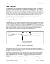
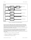
Chapter 3 Signal Connections
© National Instruments Corporation 3-27 Lab-PC+ User Manual
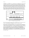
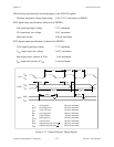
The following specifications and ratings apply to the 8253 I/O signals:
Absolute maximum voltage input rating: -0.5 to 7.0 V with respect to DGND
8253 digital input specifications (referenced to DGND):
V
IH
input logic high voltage 2.2 V minimum
V
IL
input logic low voltage 0.8 V maximum
Input load current ±10 µA maximum
8253 digital output specifications (referenced to DGND):
V
OH
output logic high voltage 3.7 V minimum
V
OL
output logic low voltage 0.45 V maximum
I
OH
output source current, at V
OH
-1 mA maximum
I
OL
output sink current, at V
OL
4 mA maximum
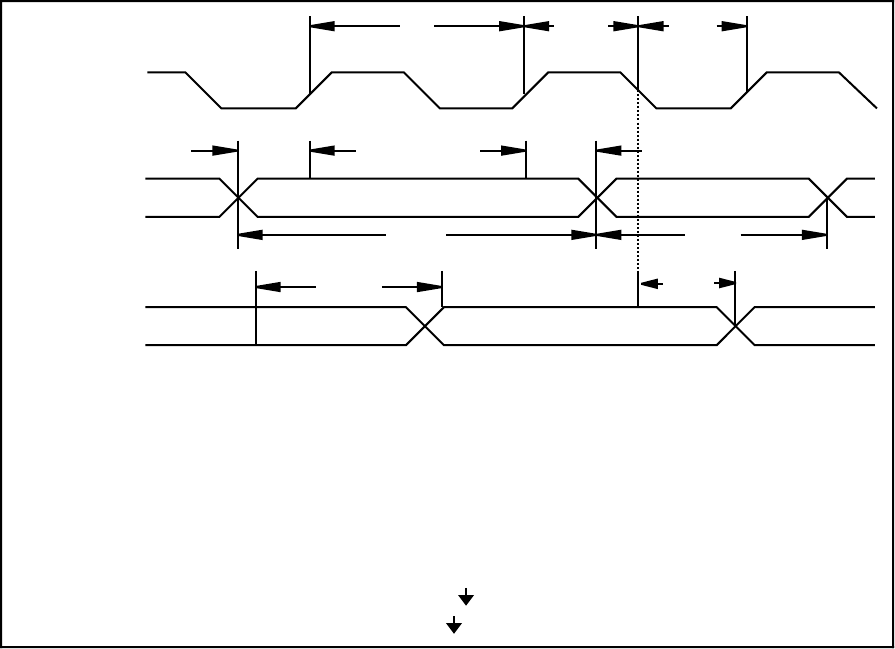
t
sc
t
pwh
t
pwl
t
gsu
t
gh
t
gwh
t
gwl
t
outc
t
outg
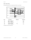
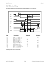
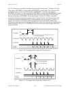
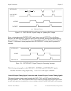
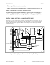
CLK
GATE
OUT
V
OH
V
IH
V
IL
V
IH
V
OL
V
IL
t
sc
t
pwh
t
pwl
t
gsu
t
gh
t
gwh
t
gwl
t
outg
t
outc
clock period
clock high level
clock low level
gate setup time
gate hold time
gate high level
gate low level
output delay from clock
output delay from gate
380 nsec minimum
230 nsec minimum
150 nsec minimum
100 nsec minimum
50 nsec minimum
150 nsec minimum
100 nsec minimum
300 nsec maximum
400 nsec maximum
Figure 3-17. General-Purpose Timing Signals