


Register-Level Programming Appendix E
Lab-PC+ User Manual E-22 © National Instruments Corporation
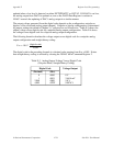
The following formula calculates the voltage output versus digital code for a bipolar analog
output configuration and two’s complement coding:
V
out
= 5.0
*
(digital code)
2,048
The digital code in the above formula is a decimal value ranging from -2,048 to +2,047. Notice
that two’s complement mode coding is selected by setting the 2SDAC bit high in Command
Register 2.
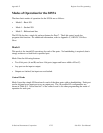
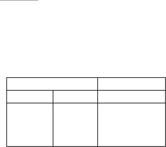
Table E-4. Analog Output Voltage Versus Digital Code
(Bipolar Mode, Two’s Complement Coding)
Digital Code Voltage Output
(Decimal) (Hex) (V
ref
= 10 V)
-2,048 F800 -5.0 V
-1,024 FC00 2.5 V
0 0000 0.0 V
1,024
2,047
0400
07FF
2.5 V
4.9976 V
Interrupt Programming for the Analog Output Circuitry
Interrupts can be used for writing successive values in a sequence to the DAC Data Registers
during a waveform generation operation. The CNTINTEN bit in Command Register 3 enables
and disables Counter A2 and EXTUPDATE* driven interrupts. See Chapter 3, Signal
Connections, for timing requirements on the EXTUPDATE* signal.
The following programming steps are required for waveform generation using interrupts:
1. Set up Command Register 2.
The LDAC0 bit must be set high for enabling OUTA2 or EXTUPDATE* driven updates on
DAC0. LDAC1 bit must be set high for enabling OUTA2 or EXTUPDATE* driven updates
on DAC1.
2. Program Counter A2.
If EXTUPDATE* is being used to update the DACs, Counter A2 output (OUTA2) must be
set high by writing B8 (hex) to the Counter A Mode Register. If OUTA2 is being used to
update the DACs, EXTUPDATE* must be left unconnected or driven to a TTL-high level.
Counter A2 must be programmed in Mode 2 with the appropriate update interval.