


Register-Level Programming Appendix E
Lab-PC+ User Manual E-4 © National Instruments Corporation
The DAVAIL bit indicates whether one or more A/D conversion results are stored in the A/D
FIFO. If the DAVAIL bit is cleared, the A/D FIFO is empty and reading the A/D FIFO Register
returns meaningless data. Once an A/D conversion is initiated, the DAVAIL bit should be set
after 12 µs or after a rising edge on OUTA0, whichever occurs later. If EXTCONV* is being
used for A/D timing, the DAVAIL bit should be set after 12 µs or after a rising edge in
EXTCONV*, whichever occurs later.
An A/D FIFO overflow condition occurs if more than 16 conversions are initiated and stored in
the A/D FIFO before the A/D FIFO Register is read. If this condition occurs, the OVERFLOW
bit is set in the Status Register to indicate that one or more A/D conversion results have been lost
because of FIFO overflow. Writing to the A/D Clear Register resets this error flag. Two 8-bit
dummy reads must be performed on the FIFO after an A/D Clear to reset the FIFO.
A/D FIFO Output Binary Modes
The A/D conversion result can be returned from the A/D FIFO as a 16-bit two’s complement or
straight binary value by setting or clearing the TWOSCMP bit in Command Register 1. If the
analog input circuitry is configured for the input range 0 to +10 V, straight binary mode should
be used (clear the TWOSCMP bit). Straight binary mode returns numbers between 0 and +4,095
(decimal) when the A/D FIFO Register is read. If the analog input circuitry is configured for the
input range -5 to +5 V, two’s complement mode is more appropriate (set the TWOSCMP bit).
Two’s complement mode returns numbers between -2,048 and +2,047 (decimal) when the A/D
FIFO Register is read.
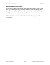
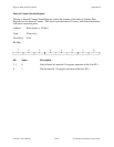
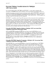
Table E-1 shows input voltage versus A/D conversion values for the 0 to +10 V input range.
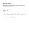
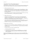
Table E-2 shows input voltage versus A/D conversion values for two’s complement mode and
-5 to +5-V input range.
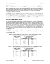
Table E-1. Unipolar Input Mode A/D Conversion Values (Straight Binary Coding)
Input Voltage
(Gain = 1)
A/D Conversion Result
Range: 0 to +10 V
(Decimal) (Hex)
0 0 0000
2.5 1,024 0400
5.0 2,048 0800
7.5 3,072 0C00
9.9976 4,095 0FFF
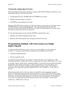
Table E-2. Bipolar Input Mode A/D Conversion Values (Two’s Complement Coding)
Input Voltage
(Gain = 1)
A/D Conversion Result
Range: -5 to +5 V
Decimal Hex
-5.0 -2,048 F800
2.5 -1,024 FC00
0 0 0000
2.5 1,024 0400
4.9976 2,047 07FF