


Appendix D Register Map and Descriptions
© National Instruments Corporation D-13 Lab-PC+ User Manual
Command Register 4
This register allows multiplexing of certain A/D conversion logic signals. This enables the
interval scanning and A/D conversion signals to be available at the I/O connector and allows the
I/O connector pins to externally drive these signals.
Address: Base address + 0F (hex)
Type: Write-only
Word Size: 8-bit
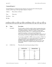
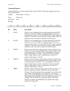
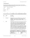
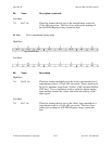
Bit Map:
765 43210
X X X ECLKRCV SE
__
/D ECLKDRV EOIRCV INTSCAN
Bit Name Description
7-5 X Don't care bits.
4 ECLKRCV When cleared, this bit enables EXTCONV* pulses applied at the
EXTCONV* pin on the connector to cause conversions when
ECLKDRV is cleared. When set, ECLKRCV inhibits
EXTCONV* pulses from causing conversions. This bit is cleared
on board reset.
3SE
__
/D This bit along with jumper W4 selects the analog input mode of the
Lab-PC+. When clear, it selects the single-ended mode. In this
case, multiplexer 1 selects Channels 0-7 specified by the channel
select bits, and multiplexer 2 selects AISENSE/AIGND. If W4 is
configured in SE mode, AISENSE/AIGND gets tied to analog
ground. This is the RSE mode. If W4 is configured as DIFF,
AISENSE/AIGND does not get tied to analog ground. This is the
NRSE mode. When this bit is set, the differential mode of input is
selected. Now W4 must be in the DIFF setting. This is the DIFF
mode. In this mode, Mux 1 and Mux 2 select channel pairs (0,1),
(2,3), (4,5) or (6,7) depending on the channel selection bits. This
bit defaults to zero on reset, thus choosing the single-ended mode.
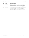
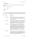
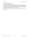
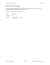
Refer to the following table for choosing the appropriate mode.
W4 Configuration SE
__
/D (Bit 3) Input Mode
RSE (A-B)
NRSE/DIFF (B-C)
NRSE/DIFF (B-C)
0
0
1
RSE (factory setting)
NRSE
DIFF