


© National Instruments Corporation 4-1 Lab-PC+ User Manual
Chapter 4
Theory of Operation
This chapter contains a functional overview of the Lab-PC+ and explains the operation of each
functional unit making up the Lab-PC+. This chapter also explains the basic operation of the
Lab-PC+ circuitry.
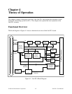
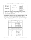
Functional Overview
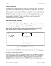
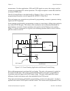
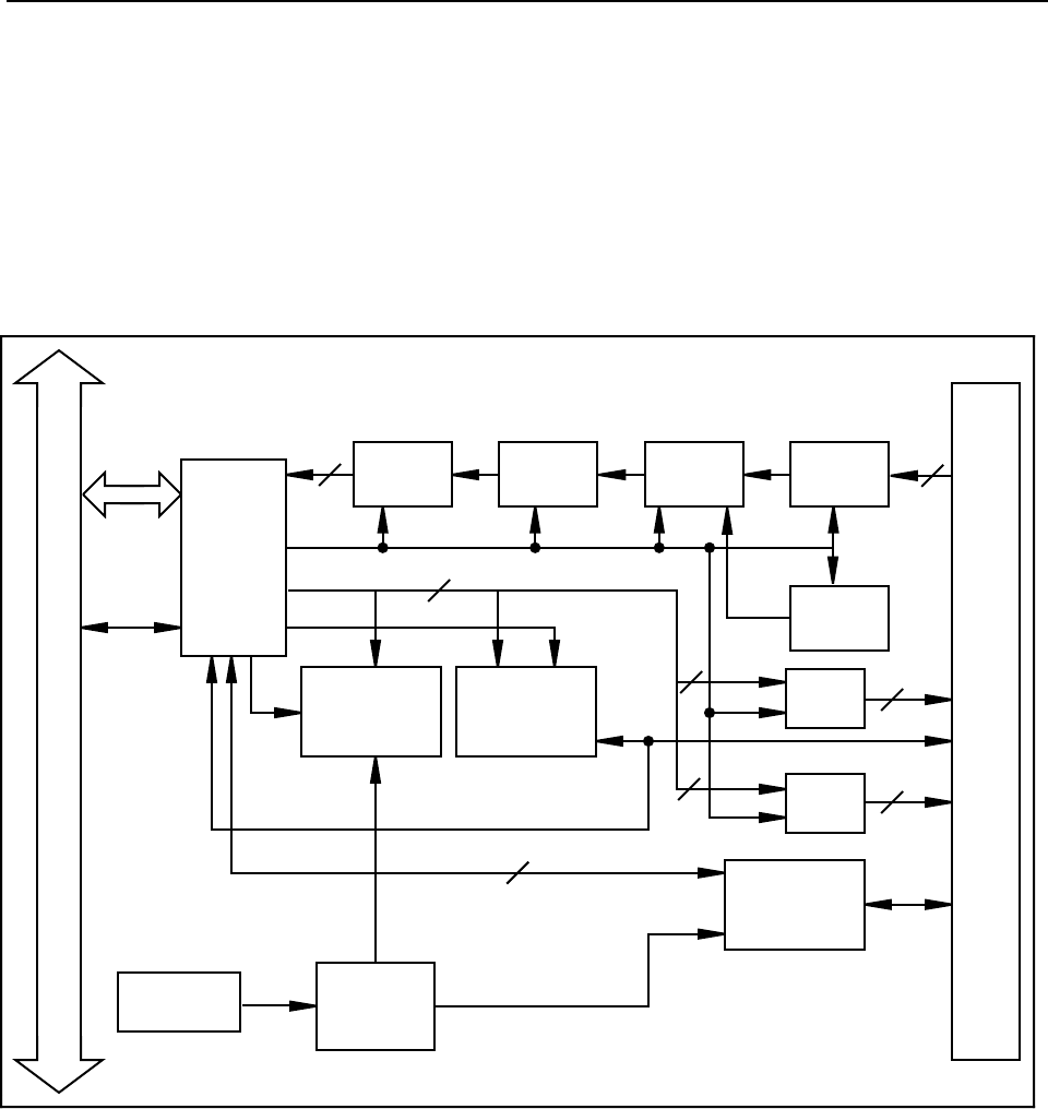
The block diagram in Figure 4-1 shows a functional overview of the Lab-PC+ board.
Data/
Address
12-Bit
D/A
12-Bit
D/A
1-MHz
Timebase
2 MHz
Timebase
Control
Signals
12
12
8
8253
Ctr/Timer
Group B
PC I/O
Channel
Interface
FIFO
16
8253
Ctr/Timer
Group A
8255A
Digital
Interface
8
Input
Mux
Pgm
Gain
12-Bit
A/D
÷ 10
÷ 5
10 MHz
Oscillator
12
1
1
PC I/O Channel
Back Panel Connector
Input
Mux
Figure 4-1. Lab-PC+ Block Diagram