


Chapter 4 Theory of Operation
© National Instruments Corporation 4-3 Lab-PC+ User Manual
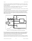
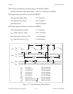
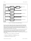
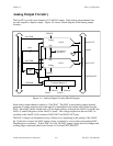
Address Bus
Address
Latches
Address
Decoder
Timing
Interface
Data
Buffers
DMA
Control
Interrupt
Control
Control Lines
Data Bus
DMA REQ
DMA ACK
IRQ
Register Selects
Read and Write Signals
Internal Data Bus
DMA Request
DMA ACK and DMATC
Interrupt Requests
PC I/O Channel
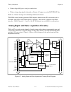
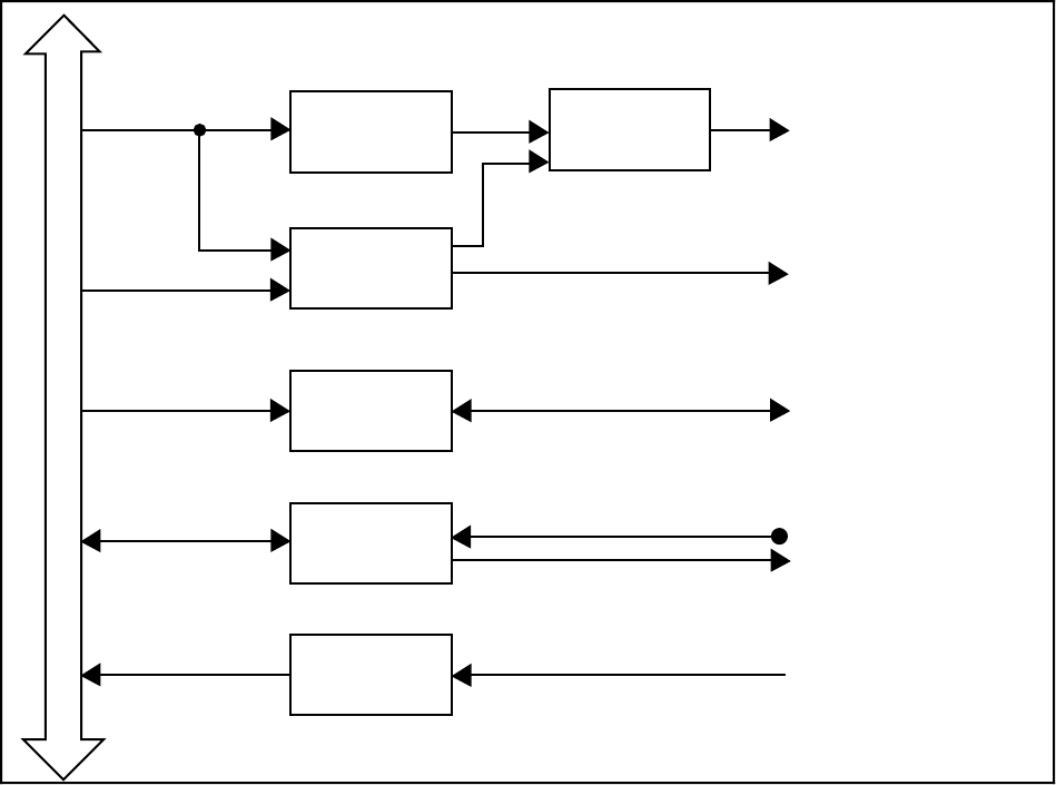
Figure 4-2. PC I/O Interface Circuitry Block Diagram
The circuitry consists of address latches, address decoders, data buffers, I/O channel interface
timing control circuitry, interrupt control circuitry and DMA control circuitry. The circuitry
monitors the address lines SA5 through SA9 to generate the board enable signal, and uses lines
SA0 through SA4 plus timing signals to generate the onboard register select signals and
read/write signals. The data buffers control the direction of data transfer on the bidirectional data
lines based on whether the transfer is a read or write.
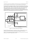
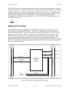
The interrupt control circuitry routes any enabled interrupts to the selected interrupt request line.
The interrupt requests are tristate output signals allowing the Lab-PC+ board to share the
interrupt lines with other devices. Six interrupt request lines are available for use by the
Lab-PC+–IRQ3, IRQ4, IRQ5, IRQ6, IRQ7, and IRQ9. Five different interrupts can be generated
by the Lab-PC+:
• When an A/D conversion is available to be read from FIFO
• When either an OVERFLOW or an OVERRUN error occurs
• When DMA terminal count pulse is received