


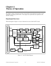
Chapter 4 Theory of Operation
© National Instruments Corporation 4-9 Lab-PC+ User Manual
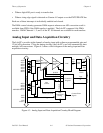
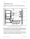
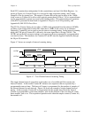
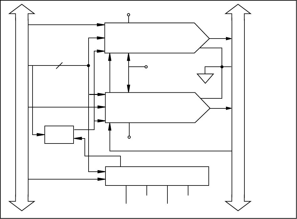
Analog Output Circuitry
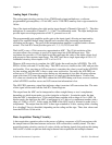
The Lab-PC+ provides two channels of 12-bit D/A output. Each analog output channel can
provide unipolar or bipolar output. Figure 4-4 shows a block diagram of the analog output
circuitry.
DAC0
DAC1
Command Register 2
Ref
Coding
Coding
Ref
DAC0 OUT
AGND
DAC1 OUT
EXTUPDATE*
5 V Internal
Reference
DAC0WR
Data
DAC1WR
Counter
A2
CNFGWR
2SDAC0
LDAC1
2SDAC1
LDAC0
2SDAC0
2SDAC1
8
I/O Connector
PC I/O Channel
Figure 4-4. Analog Output Circuitry Block Diagram
Each analog output channel contains a 12-bit DAC. The DAC in each analog output channel
generates a voltage proportional to the input V
ref
multiplied by the digital code loaded into the
DAC. Each DAC can be loaded with a 12-bit digital code by writing to the DAC0 (L and H) and
DAC1 (L and H) Registers on the Lab-PC+ board. The voltage output from the two DACs is
available at the Lab-PC+ I/O connector DAC0 OUT and DAC1 OUT pins.
The DAC voltages can be updated in any of three ways, depending on the setting of the LDAC
bit. If this bit is cleared, the DAC output voltage is updated as soon as the corresponding DAC
Data Register is written to. If the LDAC bit is set, the DAC output voltage does not change until
a falling edge is detected either from Counter A2 or from EXTUPDATE*.