


Theory of Operation Chapter 4
Lab-PC+ User Manual 4-10 © National Instruments Corporation
Each DAC channel can be jumper-programmed for either a unipolar voltage output or a bipolar
voltage output range. A unipolar output gives an output voltage range of 0.0000 V to +9.9976 V.
A bipolar output gives an output voltage range of -5.0000 V
to +4.9976 V. For unipolar output,
0.0000 V output corresponds to a digital code word of 0. For bipolar output, -5.0000 V output
corresponds to a digital code word of F800 (hex). One LSB is the voltage increment
corresponding to a LSB change in the digital code word. For both unipolar and bipolar output,
one LSB corresponds to:
10 V
4,096
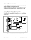
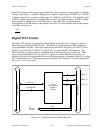
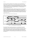
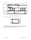
Digital I/O Circuitry
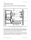
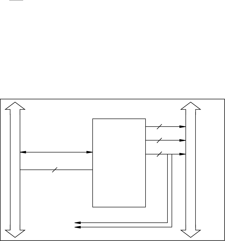
The digital I/O circuitry is designed around an 8255A integrated circuit. Figure 4-5 shows a
block diagram of the digital I/O circuitry. The 8255A is a general-purpose PPI containing
24 programmable I/O pins. These pins represent the three 8-bit I/O ports (A, B, and C) of the
8255A as well as PA<0..7>, PB<0..7>, and PC<0..7> on the Lab-PC+ I/O connector. The
8255A also has a control register to configure each of the three I/O ports on the chip. These
ports can be programmed as two groups of 12 signals or as three individual 8-bit ports. In
addition, the board can be programmed in one of the three modes of operation–basic I/O, strobed
I/O, or bidirectional bus. The programming of the digital I/O circuitry is covered in Appendix E,
Register-Level Programming.
8255A
Programmable
Peripheral
Interface
To
Interrupt
Control
DIO RD/WR
DATA<0..7>
PC0
PC3
PC<0..7>
PB<0..7>
PA<0..7>
I/O Connector
PC I/O Channel
2
8
8
8
Figure 4-5. Digital I/O Circuitry Block Diagram