


Calibration Chapter 5
Lab-PC+ User Manual 5-4 © National Instruments Corporation
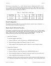
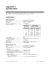
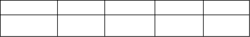
The voltages corresponding to V
-fs
, which is the most negative voltage that the ADC can read,
V
+fs
- 1, which is the most positive voltage the ADC can read, and 1 LSB, which is the voltage
corresponding to one count of the ADC, depend on the input range selected. The value of these
voltages for each input range is given in Table 5-1.
Table 5-1. Voltage Values of ADC Input
Input Range V
-fs
V
+fs
- 1 1 LSB 0.5 LSB
-5 to +5 V -5 V +4.99756 V 2.44 mV 1.22 mV
0 to 10 V 0 V +9.99756 V 2.44 mV 1.22 mV
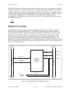
Board Configuration
The calibration procedure differs if you select either bipolar or unipolar input configuration. A
procedure for each configuration is given next.
Bipolar Input Calibration Procedure
If your board is configured for bipolar input, which provides the range -5 to +5 V, then complete
the following procedure in the order given. This procedure assumes that ADC readings are in the
range -2,048 to +2,047, that is, the TWOSADC bit in Command Register 1 is set high. The
following should be performed with the input configuration set to RSE.
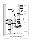
1. Input Offset Calibration
To adjust the amplifier input offset:
a. Connect ACH0 (pin 1 on the I/O connector) to AISENSE/AIGND (pin 9).
b. Take analog input readings from Channel 0 at gains of 1 and 50.
c. Adjust trimpot R7 until the readings match to within one count at both gain settings.
2. Output Offset Calibration
To adjust the amplifier output offset:
a. Connect ACH0 (pin 1 on the I/O connector) to AISENSE/AIGND (pin 9).
b. Take analog input readings from Channel 0 at the gain at which the system will be used.
c. Adjust trimpot R6 until the readings are 0 ±0.5 LSB.
Alternatively, the above offset calibration procedure can be carried out with the input gain set
at 1, followed by recording the average reading at all other gains. These readings can be used