


Theory of Operation Chapter 4
Lab-PC+ User Manual 4-14 © National Instruments Corporation
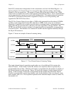
OUTB1
OUTA0
Interval
Counter
Sample
Interval
Scan
Interval
CONVERT
GATEA0
Sample
Interval
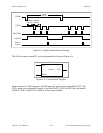
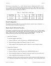
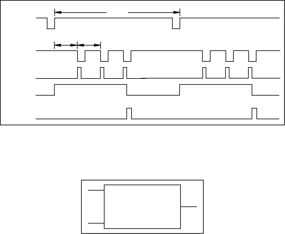
Figure 4-8. Single-Channel Interval Timing
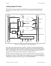
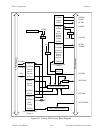
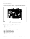
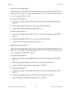
The 16-bit counters in the 8253 can be diagrammed as shown in Figure 4-9.
CLK
GATE
OUT
Counter
Figure 4-9. Counter Block Diagram
Each counter has a CLK input pin, a GATE input pin, and an output pin labeled OUT. The
8253 counters are numbered 0 through 2, and their GATE, CLK, and OUT pins are labeled
GATE N, CLK N, and OUT N, where N is the counter number.