


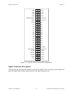
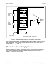
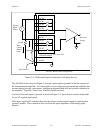
Signal Connections Chapter 3
Lab-PC+ User Manual 3-2 © National Instruments Corporation
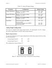
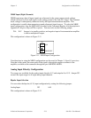
12
34
56
78
9 10
11 12
13 14
15 16
17 18
19 20
21 22
23 24
25
26
27 28
29 30
31 32
33 34
35 36
37 38
39 40
41 42
43 44
45 46
47 48
49 50
PC3
PC2PC1
PC0PB7
PB6PB5
PB4PB3
PB2PB1
PB0PA 7
PA 6PA 5
PA 4PA 3
PA 2PA 1
PA 0DGND
DAC1 OUTAGND
ACH6
ACH4
ACH2
ACH5
AISENSE/AIGND
ACH7
PC4
PC5 PC6
PC7 EXTTRIG
OUTB0
EXTCONV*
+5 V
CLKB2GATB2
OUTB2
CCLKB1
GATB1COUTB1
GATB0
DGND
DAC0 OUT
ACH1
ACH3
ACH0
EXTUPDATE*
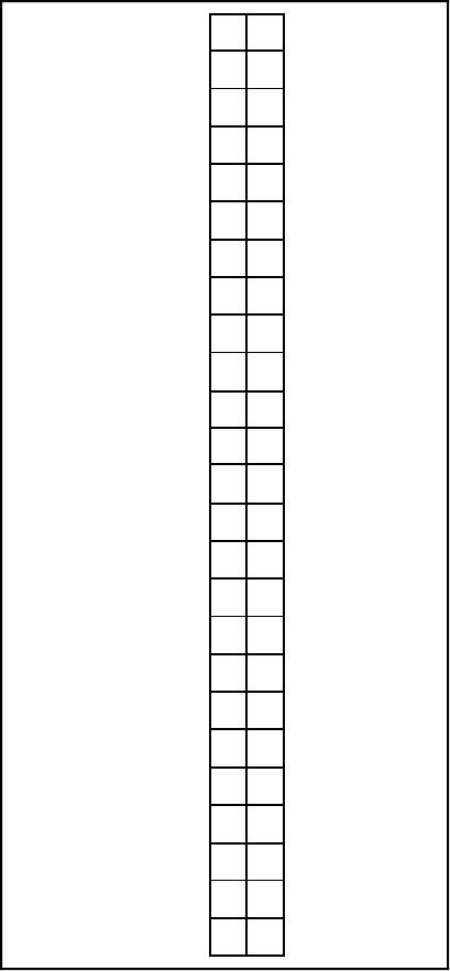
Figure 3-1. Lab-PC+ I/O Connector Pin Assignments
Signal Connection Descriptions
The following list describes the connector pins on the Lab-PC+ I/O connector by pin number and
gives the signal name and the significance of each signal connector pin.