


Signal Connections Chapter 3
Lab-PC+ User Manual 3-12 © National Instruments Corporation
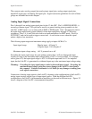
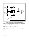
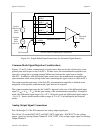
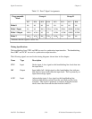
ACH 0
V
m
Measured
Voltage
Common
Mode
Noise
and so on
AGND
AISENSE/AIGND
V
s
V
cm
-
-
+
+
-
+
-
+
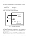
I/O Connector
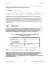
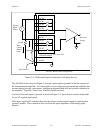
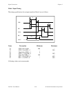
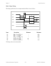
Lab-PC+ Board in NRSE Input Configuration
1
2
3
8
9
11
Ground-
Referenced
Signal
Source
ACH 1
ACH 2
ACH 7
Figure 3-6. Single-Ended Input Connections for Grounded Signal Sources
Common-Mode Signal Rejection Considerations
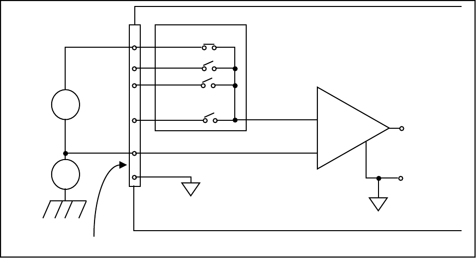
Figures 3-3 and 3-6 show connections for signal sources that are already referenced to some
ground point with respect to the Lab-PC+. In these cases, the instrumentation amplifier can
reject any voltage due to ground potential differences between the signal source and the
Lab-PC+. In addition, with differential input connections, the instrumentation amplifier can
reject common-mode noise pickup in the leads connecting the signal sources to the Lab-PC+.
The common-mode input range of the Lab-PC+ instrumentation amplifier is defined as the
magnitude of the greatest common-mode signal that can be rejected.
The common-mode input range for the Lab-PC+ depends on the size of the differential input
signal (V
diff
= V
+
in
- V
-
in
) and the gain setting of the instrumentation amplifier. In unipolar
mode, the differential input range is 0 to 10 V. In bipolar mode, the differential input range is
-5 to +5 V. Inputs should remain within a range of -5 to 10 V in both bipolar and unipolar
modes.
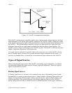
Analog Output Signal Connections
Pins 10 through 12 of the I/O connector are analog output signal pins.
Pins 10 and 12 are the DAC0 OUT and DAC1 OUT signal pins. DAC0 OUT is the voltage
output signal for Analog Output Channel 0. DAC1 OUT is the voltage output signal for Analog
Output Channel 1.