


Appendix E Register-Level Programming
© National Instruments Corporation E-23 Lab-PC+ User Manual
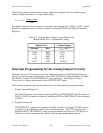
3. Enable timer interrupts.
Timer interrupts refer to the interrupts generated by rising edges on OUTA2 or
EXTUPDATE*. A rising edge on OUTA2 or EXTUPDATE* sets the CNTINT bit high in
the Status Register. A timer interrupt is generated whenever the CNTINT bit in the Status
Register and the CNTINTEN bit in Command Register 3 are set high. Set the CNTINTEN
bit in Command Register 3 high to enable timer interrupts.
Programming the Digital I/O Circuitry
The digital I/O circuitry is designed around an 8255A integrated circuit. The 8255A is a general-
purpose PPI containing 24 programmable I/O pins. These pins represent the three 8-bit I/O ports
(A, B, and C) of the 8255A. These ports can be programmed as two groups of 12 signals or as
three individual 8-bit ports. The following paragraphs include programming information for the
Lab-PC+.
The three 8-bit ports are divided into two groups: Group A and Group B (two groups of 12
signals). One 8-bit configuration (or control) word specifies the mode of operation for each
group. The control bits of Group A configure Port A (A0 through A7) and the upper 4 bits
(nibble) of Port C (C4 through C7). The control bits of Group B configure Port B (B0 through
B7) and the lower nibble of Port C (C0 through C3). These configuration bits are defined later in
this chapter.
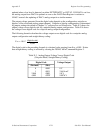
Register Descriptions and Programming Examples
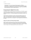
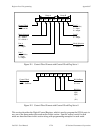
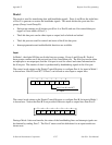
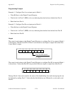
The following figures show the two control-word formats used to completely program the
8255A. The control-word flag determines which control-word format is being programmed.
When the control-word flag is 1, bits 0 through 6 specify the I/O characteristics of the 8255A's
ports and the mode in which they are operating (that is, Mode 0, Mode 1, or Mode 2). When the
control-word flag is 0, bits 3 through 0 specify the bit set/reset format of Port C.