


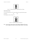

Chapter 3 Signal Connections
© National Instruments Corporation 3-3 Lab-PC+ User Manual
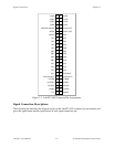
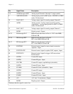
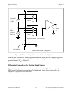
Pin Signal Name Description
1-8 ACH0 through ACH7 Analog input Channels 0 through 7 (single-ended).
9 AISENSE/AIGND Analog input ground in RSE mode, AISENSE in NRSE
mode. Bi-directional.
10 DAC0 OUT Voltage output signal for analog output Channel 0.
11 AGND Analog ground. Analog output ground for analog
output mode. Analog input ground for DIFF or NRSE
mode. Bi-directional.
12 DAC1 OUT Voltage output signal for analog output Channel 1.
13 DGND Digital ground. Output.
14-21 PA0 through PA7 Bidirectional data lines for Port A. PA7 is the MSB,
PA0 the LSB.
22-29 PB0 through PB7 Bidirectional data lines for Port B.
PB7 is the MSB, PB0 the LSB.
30-37 PC0 through PC7 Bidirectional data lines for Port C.
PC7 is the MSB, PC0 the LSB.
38 EXTTRIG External control signal to start a timed conversion
sequence. Input.
39 EXTUPDATE* External control signal to update DAC outputs. Input.
40 EXTCONV* External control signal to trigger A/D conversions.
Bi-directional.
41 OUTB0 Counter B0 output.
42 GATB0 Counter B0 gate. Input.
43 COUTB1 Counter B1 output or pulled high (selectable).
44 GATB1 Counter B1 gate. Input.
45 CCLKB1 Counter B1 clock (selectable). Input.
46 OUTB2 Counter B2 output.
47 GATB2 Counter B2 gate. Input.
48 CLKB2 Counter B2 clock. Input.
49 +5V +5 V out, 1 A maximum. Output.
50 DGND Digital ground. Output.
*Indicates that the signal is active low.