


Bus Controller (BC)
8-3
8.3 Bus Configuration
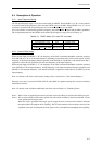
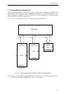
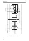
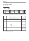
Fig. 8-3-1 shows the bus configuration. The chip’s internal buses are the ROM bus between the CPU core and
internal instruction ROM/internal flash memory, the RAM bus between the CPU core and internal data RAM, the
BC bus between the CPU core and the bus controller, and the I/O bus between the bus controller and internal I/O.
The EX bus is an external bus.
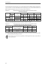
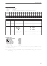
Table 8-3-1 lists the characteristics of each bus.
Fig. 8-3-1 Bus Configuration Diagram
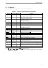
Table 8-3-1 Characteristics of Each Bus
Bus name Blocks Data bus width Operating clock
ROM bus CPU - internal instruction ROM/ 64 MCLK
(*1)
internal flash memory
RAM bus CPU - internal data RAM 32 MCLK
(*1)
BC bus CPU - BC 32 MCLK
(*1)
I/O bus BC - internal I/O 32 IOCLK
(*1)
[synchronous mode]
EX bus BC - external memory 8/16
(*2)
SYSCLK
(*1)
[synchronous mode]
(external bus) MCLK
(*1)
[asynchronous mode]
(*1) For a description of the operation clock, refer to section 8.8, “Operation Clock.”
(*2) Set by the external input pin or control register.
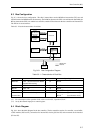
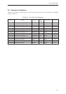
8.4 Block Diagram
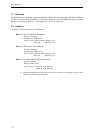
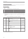
Fig. 8-4-1 shows the block diagram for the bus controller. The bus controller consists of a controller, a store buffer,
a CPU interface (BC bus I/F), an interface for internal I/O circuitry (I/O bus I/F) and an external device interface
(EX bus I/F).
Address bus
Data bus
External
memory
I/O bus
32
CPU core
Bus controller
BC bus
32
Internal I/O
(peripherals)
32
24
EX bus
8/16
RAM bus
32
Internal
Data RAM
(8 KB)
DRAM I/F
Store buffer
External memory
interface
ROM bus
64
Internal
instruction ROM
(128 KB)/Internal
flash memory
(256 KB)