


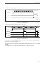
Serial Interface
13-25
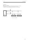
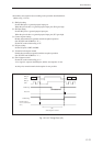
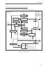
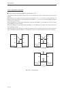
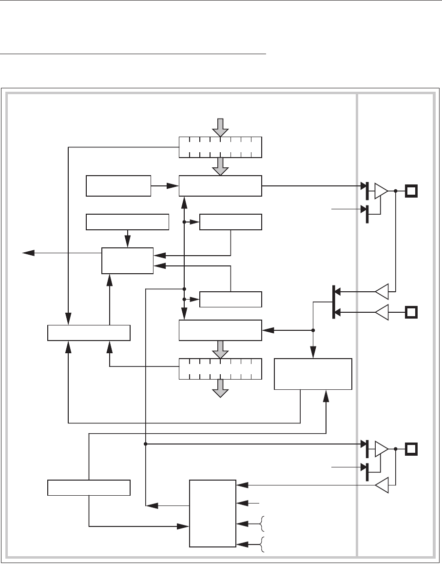
13.3.2 Block Diagram of Clock Synchronous Serial Interface
Fig 13-3-1 shows the block diagram for the clock synchronous serial interface sections.
Fig. 13-3-1 Block Diagram
Transmission buffer
Shift register
SBIn
SBTn
Reception buffer read
Transmission buffer write
Parity bit check
Parity bit addition
Transfer
clock
control
IOCLK
Transfer
clock
Reception buffer
Shift register
Interrupt request
generation
Transmission
interrupt request
Reception
interrupt request
Serial interface n
(n = 1, 2)
Timer 2 underflow when n = 1
Timer 3 underflow when n = 2
Timer 8 underflow when n = 1
Timer 9 underflow when n = 2
Transmission bit
counter
Reception bit
counter
SCnCTR
Control register
SCnSTR
Status register
SCnICR
Interrupt mode register
SBOn
Output control
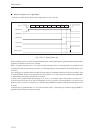
I/O Port Block
Set the serial signals in
the I/O port control
register. However, some
pins may need to be set
as general-purpose
inputs, depending on the
transmission/reception
procedure.
Output control