


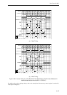
Bus Controller (BC)
8-59
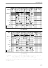
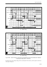
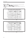
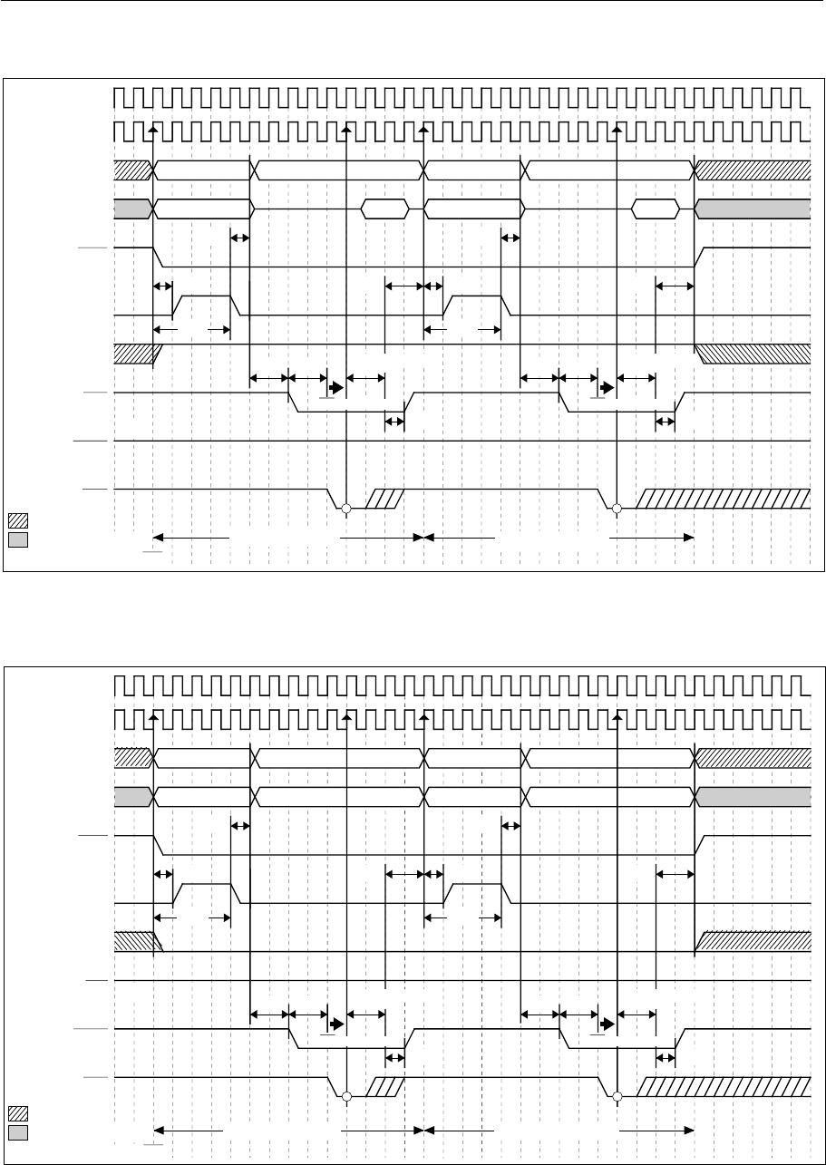
(a) Read Timing
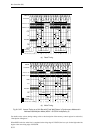
(b) Write Timing
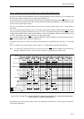
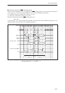
Fig. 8-13-29 Access Timing on a 8-bit Bus with Handshaking in Synchronous Mode and in Address/
Data Multiplex Mode (MCLK = SYSCLK)
For details on the various timing settings, refer to the description of the memory control register in section 8.6,
“Description of Registers.”
MCLK
SYSCLK
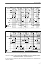
AS
CS2
ASA
ADE
RWSEL
A23* to 16
ADM15 to 0
RE
WE0
ASN
ASA
ADE
ASN
EA
REN
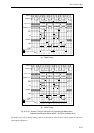
Read high-order side
Read low-order side
DK
DW
BCE BCE
EA
REN
DW
DK detection startDK detection start
A[0]=0 A[0]=1
data in data in
“H”
A[0]=0
A[0]=1
: Undefined
Consumed internally
by the BC
Consumed internally
by the BC
: A23 also serves as CS3
*
: Undefined or Hi-Z
“0” (“L”)
“0” (“L”)
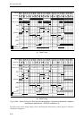
MCLK
SYSCLK
AS
CS2
ASA
ADE
RWSEL
A23* to 16
ADM15 to 0
RE
WE0
ASN
ASA
ADE
ASN
EA
WEN
Write high-order side
Write low-order side
DK
DW
BCE
Consumed internally
by the BC
BCE
EA
WEN
DW
DK detection start
“H”
A[0]=0
“0” (“L”)
data out
A[0]=0
A[0]=1
A[0]=1
data out
: Undefined
: A23 also serves as CS3
*
: Undefined or Hi-Z
“0” (“L”)
Consumed internally
by the BC
DK detection start