


Bus Controller (BC)
8-40
An
D7-0
WE0
RE
CSn
MCLK
SYSCLK
Read low-
order side
Read high-
order side
Write low-
order side
Write high-
order side
A[0]=0
BCE
BCS
A[0]=1
BCE
BCS
A[0]=0
BCE
BCS
A[0]=1
BCE
BCS
EA
REN
EA
REN
EA
WEN WEN
EA
: Undefined
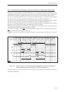
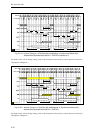
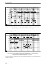
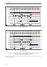
Fig. 8-13-11 Access Timing on a 8-bit Bus with Fixed Wait States, in Synchronous Mode and in
Address/Data Separate Mode (MCLK = SYSCLK multiplied by 2)
For details on the various timing settings, refer to the description of the memory control register in section 8.6,
“Description of Registers.”
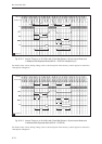
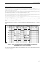
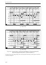
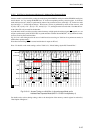
Fig. 8-13-12 Access Timing on a 8-bit Bus with Fixed Wait States, in Synchronous Mode
and in Address/Data Separate Mode (MCLK = SYSCLK)
For details on the various timing settings, refer to the description of the memory control register in section 8.6,
“Description of Registers.”
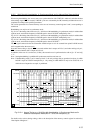
An
D7-0
WE0
RE
CSn
MCLK
SYSCLK
Read low-
order side
Read high-
order side
Write low-
order side
Write high-
order side
BCE
BCS=0
EA
REN
EA
REN
EA
EA
A[0]=0 A[0]=1
BCE BCE
BCS=0 BCE
A[0]=0
A[0]=1
WEN
WEN
: Undefined