


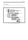


16-bit Timers
11-11
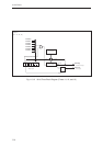
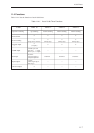
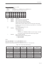
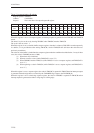
Timer n mode register (n = 11, 12, 13)
Register symbol: TMnMD
Address: x'34001082 (n=11), x'34001084 (n=12), x'34001086 (n=13)
Purpose: This register controls the operation of timer n.
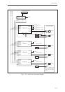
Bit No.76543210
Bit TMn TMn
–––
TMn TMn TMn
name CNE LDE CK2 CK1 CK0
Reset 0 0 0 0 0 0 0 0
Access R/W R/W R R R R/W R/W R/W
Bit No. Bit name Description
0 TMnCK0 Timer n clock source selection flag (LSB)
1 TMnCK1 Timer n clock source selection flag
2 TMnCK2 Timer n clock source selection flag (MSB)
These bits select the clock source for the timers.
When pin input is selected, counting occurs at the rising edge of the pin input.
For details on the clock sources for each timer, refer to Table 11-5-2, "16-bit Timer
Clock Sources".
5 to 3 — "0" is returned when these bits are read.
6 TMnLDE Timer n initialization flag
Initializes timer n.
0: Normal operation
1: Initialize
Loads the value in TMnBR into TMnBC, resets timer output n, and loads
the value in the compare register buffer into the compare register.
7 TMnCNE Timer n operation enable flag
Enables/disables the timer n counting operation.
0: Operation disabled.
1: Operation enabled.
[Note]
When setting TMnCNE to "1", do so while TMnLDE is set to "0".
When setting TMnLDE to "1", do so while TMnCNE is set to "0".
Operation is not guaranteed if TMnCNE and TMnLDE are both set to "1" at the same time.
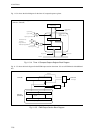
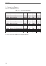
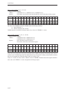
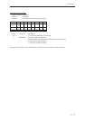
Table 11-5-2 16-bit Timer Clock Sources
TMnCK [2:0]
Timer 10 Timer 11 Timer 12 Timer 13
Setting value
000 IOCLK IOCLK IOCLK IOCLK
001 IOCLK/8 IOCLK/8 IOCLK/8 IOCLK/8
010 IOCLK/32 IOCLK/32 IOCLK/32 IOCLK/32
011 Setting prohibited Setting prohibited Setting prohibited Setting prohibited
100 Timer 0 underflow Timer 0 underflow Timer 0 underflow Timer 0 underflow
101 Timer 1 underflow Timer 1 underflow Timer 1 underflow Timer 1 underflow
110 Timer 2 underflow Timer 2 underflow Timer 2 underflow Timer 2 underflow
111 TM10IOB pin input TM11IO pin input TM12IO pin input TM13IO pin input